So NTC is working properly, glad about that. If it is still undercompensated with 220 ohm, than try a little lower value ie. 180 ohm. Without serial compensation resistor it is always overcompensated.
Thanks. With the 220 Ohm resister shorted, compensation seems very good. I adjusted the driver bias to about 10mA warm, and output offset within 5mV. I then shut off power and allowed everything to cool completely.
Upon cold start up, the driver current quickly ramps to about 7.5mA, then rises over the next 20 seconds or so to about 9.5mA. After a couple more minutes, it rises to 10.0mA and stays there. Output offset wanders a little but less than +/- 15mA. Square waves look very good - no overshoot, with a very small amount of hF noise visible in the leading edge, at 100kHz (may be due to all the probes I have connected, or may have to adjust the HF compensation a bit?).
The temporary heatsink that I'm using for the output devices is barely adequate, so it gets fairly hot, but not too hot to touch. Only the outputs are mounted on this sink. The board you see in the picture is about 1.5cm above the output sink. As the outputs heat up, the driver bias drops to about 9.5mA. So it looks like no resistor or a maybe a small one is all that is required for this version. Yes, I believe that with no series resistor it is overcompensated for the input bias drift, but that overcompensation is needed to take care of the driver thermal drift, which is otherwise not compensated for.
As I noted before, the drivers in this version are not cascaded, so there is significant power dissipated. And the driver bias is visibly sensitive to driver temperature. I have a small square of aluminum as heat radiators for the drivers (about 1mmx1.5cmx1.5cm). If I put a finger on the driver sink (they are warm to the touch, but not hot) the bias immediately begins to drop and the offset climbs.
My analysis could be completely wrong, but the result is nevertheless good.
Sheldon
The BJT version of SSA posted here earlier shows as expected very unfortunate sensitivity to complex loads.
The simulation of a 2 way speaker is accurate within 95% of the measured complex impedance of the actual speaker. A critical situation for amps sensitive to reactive distortion is around 330 Hz. There the thd of the amp jumps sharply from less than 0.03% to above 0.6% and such is audible.
Harmonic Frequency Fourier Normalized Phase Normalized
Number [Hz] Component Component [degree] Phase [deg]
1 6.000e+01 2.378e+01 1.000e+00 -0.01° 0.00°
2 1.200e+02 2.606e-03 1.096e-04 -100.19° -100.18°
3 1.800e+02 1.418e-03 5.964e-05 13.05° 13.06°
4 2.400e+02 3.070e-04 1.291e-05 99.87° 99.88°
5 3.000e+02 1.042e-04 4.383e-06 33.05° 33.06°
6 3.600e+02 6.801e-05 2.860e-06 36.28° 36.29°
7 4.200e+02 1.450e-04 6.097e-06 -2.20° -2.19°
8 4.800e+02 7.435e-05 3.127e-06 -48.58° -48.56°
9 5.400e+02 6.682e-05 2.811e-06 -54.96° -54.95°
Total Harmonic Distortion: 0.012578%
but
Harmonic Frequency Fourier Normalized Phase Normalized
Number [Hz] Component Component [degree] Phase [deg]
1 3.300e+02 2.341e+01 1.000e+00 0.59° 0.00°
2 6.600e+02 4.036e-02 1.724e-03 116.46° 115.87°
3 9.900e+02 1.246e-01 5.323e-03 113.17° 112.59°
4 1.320e+03 2.305e-02 9.845e-04 43.14° 42.55°
5 1.650e+03 4.954e-02 2.116e-03 60.91° 60.32°
6 1.980e+03 2.034e-02 8.691e-04 -11.28° -11.87°
7 2.310e+03 1.878e-02 8.023e-04 -18.24° -18.82°
8 2.640e+03 1.905e-02 8.138e-04 -58.65° -59.24°
9 2.970e+03 1.793e-02 7.659e-04 -128.37° -128.96°
Total Harmonic Distortion: 0.627743%
Attachments

It would be of interest to all of us, if you can verify in sim following tips to lower distortion in SSA:
- replace R26, R27 with CCS
- reduce R1, R2 to 100 ohm and R20, R21 proportionally, to maintain desired voltage gain
- reduce R9, R10 to few ohms to higher OLG
- cascode Q6, Q7
As partial solutions these tips were reported frequently as advancement but I don't remember if ever all of them simultaneously.
Regards Andrej 😉
Actually ur last posted diagram does not have part numbers . . . .
Perhaps it's best to post a diagram with the question - if you want to ask questions about part numbers otherwise we can spend hours hunting through the thread and still may not find the diagram you had in mind . . . .
Perhaps it's best to post a diagram with the question - if you want to ask questions about part numbers otherwise we can spend hours hunting through the thread and still may not find the diagram you had in mind . . . .
It would be of interest to all of us, if you can verify in sim following tips to lower distortion in SSA:
- replace R26, R27 with CCS
- reduce R1, R2 to 100 ohm and R20, R21 proportionally, to maintain desired voltage gain
- reduce R9, R10 to few ohms to higher OLG
- cascode Q6, Q7
As partial solutions these tips were reported frequently as advancement but I don't remember if ever all of them simultaneously.
Regards Andrej 😉
I have already reduced R1 R2 to 110 ohms and changed R20 R21 thus that full power is with 1.5 volts input, but that doesn't change the reactive distortion. I oticed further the op of the Vas is too low with roughly 4 mA
it should be 20 mA where ß/Ic linearity is good and ft is max.
I will also try to set the op of the predriver to 10 mA for the same reason because all planar BJTs of this size have their max ft at 10mA and also the max linearity ß/ic.
Will try CCS but am not convinced. We'll see.
Will try CCS but am not convinced. We'll see.
I think the basic topology is tremendous. You have attacked the output in a unique manner..where you aim to remove the P to N differences. I have fitted a current dumping error correction circuit on the version I have built. which by the way sounds rather ok...
Now to the house keeping. I do believe that the weakest part of this fine circuit and the very reason why it does not simulate particularly well is the poor relations between the impedance of the current drive and the feedback currents. The basic amp is basically fed from a 1Kohm current source..which is way too low to prevent the feedback currents from modulating the drive-current. This is the main source of error in the circuit and by fitting high (very high) impedance current-sources specs are terrific. I will not show my housekeeping here....But I'am quite sure you catch the direction.
😉
please give link for the diagram you refer to - thx 🙂
I am sorry mikelm, I apologize, I thought you were asking hahfran.
Well the parts I was comment are from hahfran's sch posted above in post #2343.
Thx Andrej 🙂
For my next point . . .
Hahfran
Your diagram is so low resolution I cant see the details - can you post a higher res version - thx 🙂
For my next point . . .
Hahfran
Your diagram is so low resolution I cant see the details - can you post a higher res version - thx 🙂
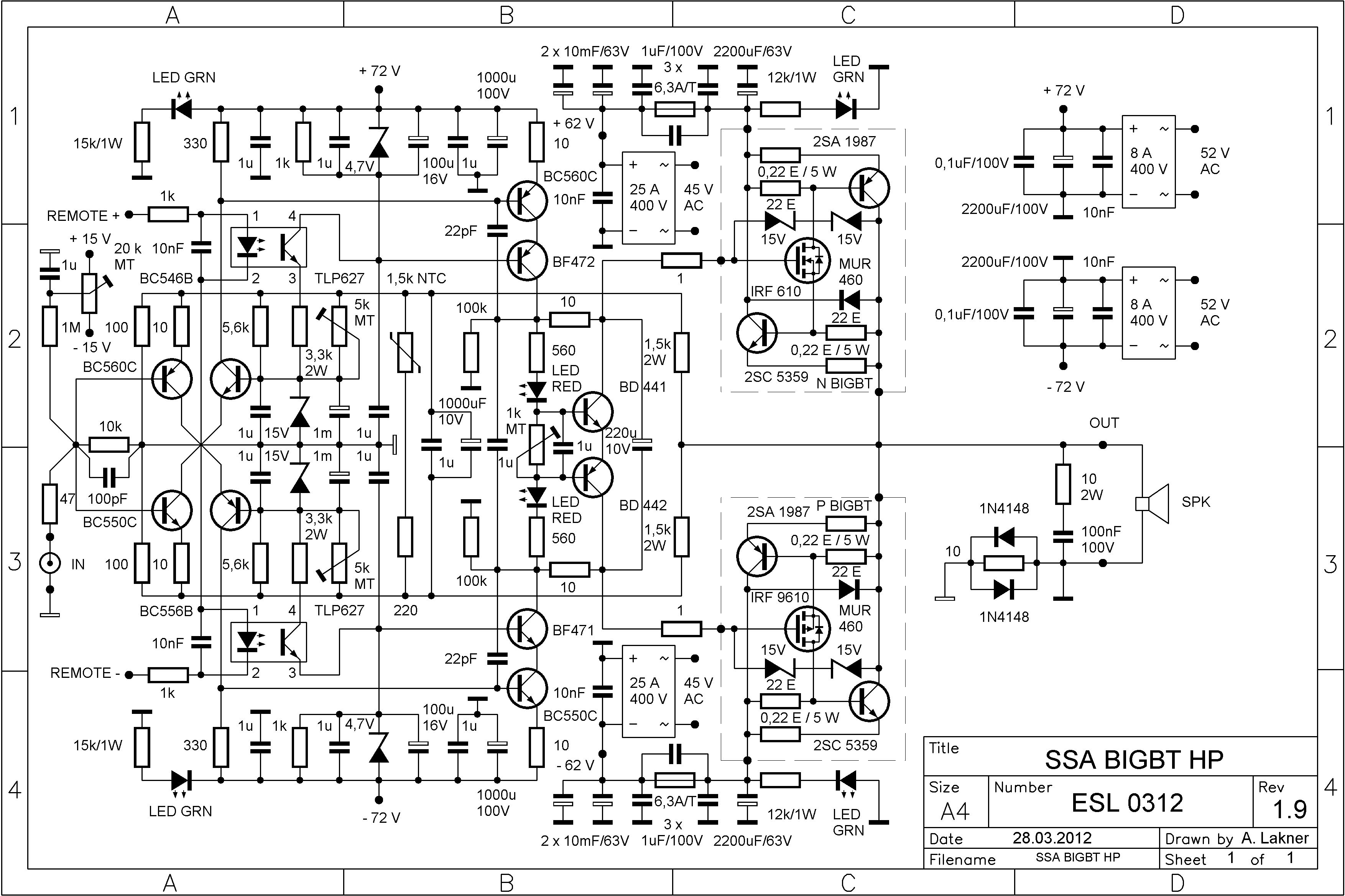
The schematics were published in this thread by lazy cat no changes made except for the complex load.
By grounding the global feedback loop thus the predriver and Vas have only local feedback
I found
the biggest source of distortion are the Vas and the power section, the latter adds high harmonics.
Adjusting R7 R8 thus that i Q6 Q7 is 20 mA and adjusting VR1 VR2 thus that offset is a few µV and i Q8 Q9 is 88 mA the open loop thd drops from 22% to 3%
Harmonic Frequency Fourier Normalized Phase Normalized
Number [Hz] Component Component [degree] Phase [deg]
1 3.300e+02 1.950e+01 1.000e+00 3.84° 0.00°
2 6.600e+02 3.218e-01 1.650e-02 -110.87° -114.72°
3 9.900e+02 3.513e-01 1.801e-02 94.46° 90.61°
4 1.320e+03 7.989e-02 4.096e-03 38.60° 34.76°
5 1.650e+03 7.843e-02 4.021e-03 47.52° 43.68°
6 1.980e+03 8.124e-02 4.166e-03 -4.96° -8.81°
7 2.310e+03 1.150e-01 5.896e-03 -98.67° -102.51°
8 2.640e+03 8.724e-02 4.473e-03 -47.22° -51.06°
9 2.970e+03 1.632e-01 8.368e-03 -147.72° -151.56°
Total Harmonic Distortion: 2.777863%
thus it is a delicate matter of setting the op of the predriver and Vas. Especially the odd harmonics are significantly reduced but still too high. Next will be setting the op of the prediver cascodes from 3mA to 10 mA.
I found the biggest source of distortion are the Vas and the power section, the latter adds high harmonics.
VAS and OPS coupling is delicate in majority of amp designs; impedance matching, feedback phase-frequency compensation, proper biasing, etc., many important factors have to be considered here. Triple output stage is also delicate by definition, enormous current gain versus stability on different ends have to meet. Best measured results don't necessarily/automatically means the best sound is achieved. 🙄
Hahfran the effort involved will bear fruit at the end for sure. 😉
. Next will be setting the op of the prediver cascodes from 3mA to 10 mA.
That works but not quite in the desired direction. The even harmonics are reduced, but odd harmonics are at best unaffected or even increase.
I'll give the topology below a try.
Of course the triple output stage has now to be inverting.
Attachments

The basic amp is basically fed from a 1Kohm current source..which is way too low to prevent the feedback currents from modulating the drive-current. This is the main source of error in the circuit and by fitting high (very high) impedance current-sources specs are terrific. I will not show my housekeeping here....But I'am quite sure you catch the direction.
Hi MiiB 😉
Today I played & messed with different CCS-s to find the most suitable one to replace my trivial FB bridge current injection resistors. The aim was not only to find the highest impedance/frequency ratio but also the best DC current/temperature stability and also lowest noise possible CCS. The winner is shown in attached schematic, which also has among the best performance/parts-count ratio. Now I only have to make four of them (two CCSources and two CCSinks) on a separete small PCB-s and install them in SSA BIGBT HP. 😉
P.S. Dynamic measurements were also performed with load resistor plus serially connected waveform/signal generator. There was practicaly no voltage modulation on load resistor, less than 0,5 mVrms up to 100 kHz at full WSG swing of 5 Vrms.
Attachments

Last edited:
Hi MiiB 😉
Today I played & messed with different CCS-s to find the most suitable one to replace my trivial FB bridge current injection resistors. The aim was not only to find the highest impedance/frequency ratio but also the best DC current/temperature stability and also lowest noise possible CCS. The winner is shown in attached schematic, which also has among the best performance/parts-count ratio. Now I only have to make four of them (two CCSources and two CCSinks) on a separete small PCB-s and install them in SSA BIGBT HP. 😉
P.S. Dynamic measurements were also performed with load resistor plus serially connected waveform/signal generator. There was practicaly no voltage modulation on load resistor, less than 0,5 mVrms up to 100 kHz at full WSG swing of 5 Vrms.
Look how busy lazy cat and boscoe (tssa) is!! They could not sleep as the ssa is spinning in there heads.

LC, I'm been searching through alot of website, the only good VAS transistor candidate are as below : 2SA1209/2SC2911, 2SA1360/2SC3423, 2SA1541/2SC3955
However, the source is from ebay, so i'm kinda risky of genuinity. Which one is better for VAS ?
About last time my destruction by spike/surge, only the Transistor are destroyed of positive portion. Negative is unharmed at all. 2 BC560C of Input and 2SA1707 for VAS, are either shorted or fused, one of them can see one piece chipped away from the transistor.
I want to ask upon your advise, that how to prevent such destruction. Does voltage regulation will safe them, by using resistor and zener only , or using 2N5401/2N5551 for cascode will do the job ? For input only, since VAS i'm going to change either one of them of above.
LC, is this CCS to replace the 3.3k resistor in your schematic on page 224? As I see it, the 3.3k resistor will pass about 15mA current, to a 15V zener.
The current source shown above is for 8,6mA, and cannot supply that current at 15V. Have you reduced the voltage for the bridge, and/or are the zeners omitted ?
Sheldon
The current source shown above is for 8,6mA, and cannot supply that current at 15V. Have you reduced the voltage for the bridge, and/or are the zeners omitted ?
Sheldon
Last edited:
LC, is this CCS to replace the 3.3k resistor in your schematic on page 224? As I see it, the 3.3k resistor will pass about 15mA current, to a 15V zener.
The current source shown above is for 8,6mA, and cannot supply that current at 15V. Have you reduced the voltage for the bridge, and/or are the zeners omitted ?
Sheldon
No, look here, 8,6 mA CCS replaces 5k6 resistor parallel to 5 k/MT trimmer. CCS supplies/inject constant current to feedback bridge from 15 V potential, previously done by resistor/trimmer. In such a way feedback bridge potential cannot change/modulate injected current, wich is actually collector drive current for input BJT-s. What's left is clear sum/subtraction between feedback current and constant drive current. The result is clear spectral components without modulated side bands. 😉
15 V zeners are not omitted, they provide stabile potential for input cascodes, plus they from reference potential for CCS-s. 😉
Last edited:
- Status
- Not open for further replies.
- Home
- Amplifiers
- Solid State
- Simple Symetrical Amplifier