sir can you re design your qusai with a op amp input?
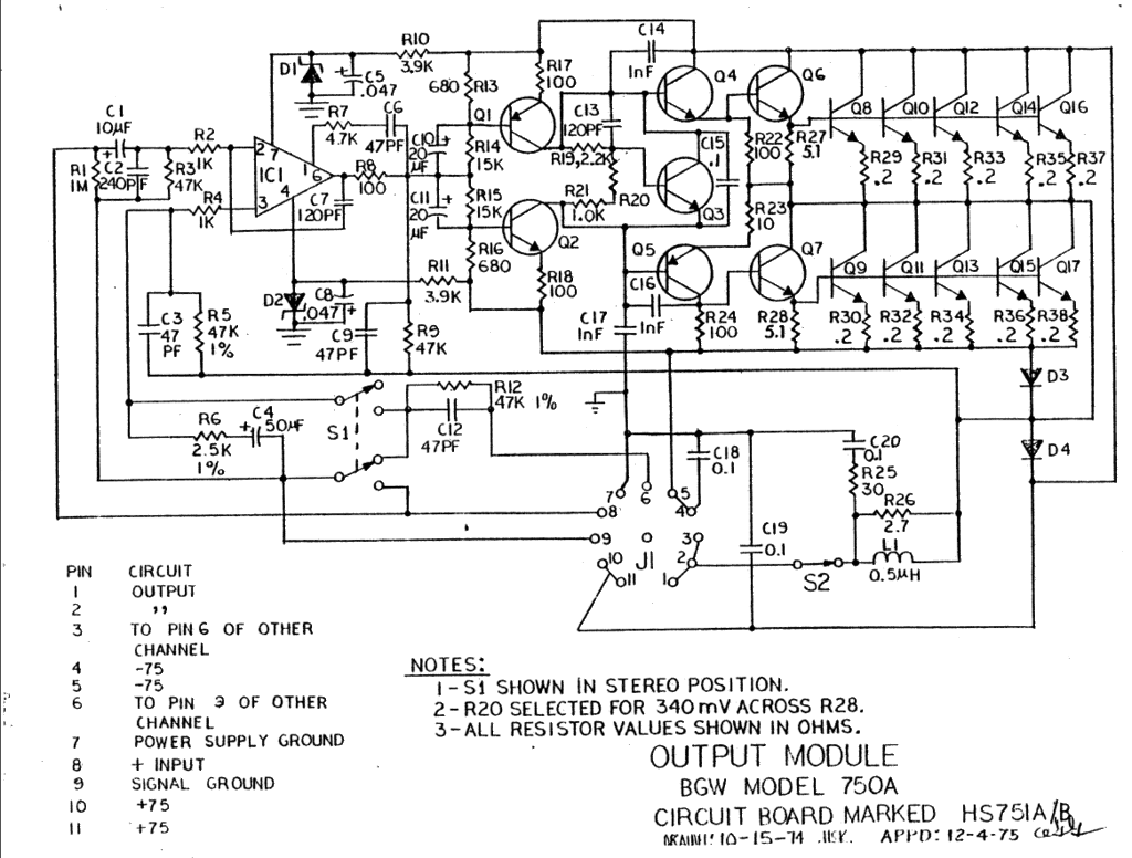
Q1, 2, 4, 5 2N3440/5415 or MJE 340/350
Bias transistor, just about anything.
Outputs (and drivers) 2N3773, MJ15022/24, etc.
Opamp LM318
Protection was a DC crowbar, a thermal cut-out on the heatsink, and a circuit-breaker on the transformer primary.
have this amp as quasi and complementary model 750 B
"Go to post #273. "
Yes, but the BGW is much simpler, and the parts are easier to find.
"have this amp as quasi and complementary model 750 B "
I have a few 250, 500D, 500R, and various 750 models. Old workhorses for sure.
Simpler than Peavey, but not simpler than APEX550. I suggest You to build BGW clone if you like it.
Regards
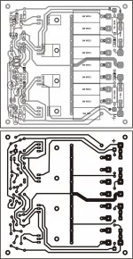
God gracious Apex, this is a great success. I made it and it works fine. Thanks you very much for the schematics and the PCB layout. Even tough I modified it a bit but it still retain the same artwork as yours. Thanks again. Below are the images:
I am using ExpressPCB for the PCB layout and the schematic. You can download it for free from this website: ExpressPCB - Free PCB layout and schematic software
please post your pcb design in pdf format.
Later BGW designs have same schematic but add VI Limiter,
if you like quasi amp Design
I suggest you to use design quasicomplementary design from DIY Member
"Quasi"
you can find it under Thread "power amp under development"
and..... BGW 750A and 750B sounding much better compare to a lot of Professional Class D Amplifier.
Have test before some weeks Class D amp with IRS2092 IC V/s old BGW 750B
No way,...BGW kick Class D amp out of the job, Class D amps are very good in effeciency but no way in premium sound
Finally: If you want better sounding amp as BGW use quasicomplementary design from DIY Member "Quasi"
hi apex,i have made pcb for this amp.Now i am about to place components.At my place a1943/c5200 & mje15030/15031 pair is available for same price i.e.2 $,so is it not fair to use these as drivers.Kindly reply me because i have bought all components except drivers.
2 SC4793 and 2 SA1837 should be possibile too as driver
can i use tip41/42 as drivers with the supply of +/-70 volts ?
No TIP41/42 can't be use, but 2SC4793 and 2SA1837 can.
Last edited:
hi apex, i have completed this amp through self made pcb.it is working fine ,currently only with +/-12 volt.pcb track for ccs mje340 base resistor is wrong in your pcb layout.
with this supply there is offset voltage of 32millivolt on output, is it right.I will increase the supply voltage after confirming about offset voltage.which set of in4148 diodes are placed on heatsink for thermal bias control ?
with this supply there is offset voltage of 32millivolt on output, is it right.I will increase the supply voltage after confirming about offset voltage.which set of in4148 diodes are placed on heatsink for thermal bias control ?
hi apex, i have completed this amp through self made pcb.it is working fine ,currently only with +/-12 volt.pcb track for ccs mje340 base resistor is wrong in your pcb layout.
with this supply there is offset voltage of 32millivolt on output, is it right.I will increase the supply voltage after confirming about offset voltage.which set of in4148 diodes are placed on heatsink for thermal bias control ?
PCB with corrected track layout, offset is high but OK, no need to place 1N4148 to heatsink this is class B amplifier. Can you post pictures?
Regards
Attachments
look at SOA.
DC is 300mA @ 75Vce. 5ms is ~900mA @ 75Vce.
After temperature de-rating would that be sufficient for reactive loads?
hi apex, i have completed this amp through self made pcb.it is working fine ,currently only with +/-12 volt.pcb track for ccs mje340 base resistor is wrong in your pcb layout.
with this supply there is offset voltage of 32millivolt on output, is it right.I will increase the supply voltage after confirming about offset voltage.which set of in4148 diodes are placed on heatsink for thermal bias control ?
Test amplifier with +/-12V rail voltage is wrong. Use 10R instead fuses or serial bulb 100W/220V in transformer primary for test, and use proper rail voltage.
Regards
"After temperature de-rating would that be sufficient for reactive loads? ?
May be marginal.
Have you looked at the MJE 15030/31 SOA? Looks like 150mA at 70V.
http://www.onsemi.com/pub_link/Collateral/MJE15028-D.PDF
I would prefer to see a triple (as used in Crown, BGW, Phase Linear, etc). Beta droop takes bites out of the 2nd and 4th quadrants of a sine wave when the driver runs out of current.
here is the photo
An externally hosted image should be here but it was not working when we last tested it.
- Home
- Amplifiers
- Solid State
- QUASI Amplifier for Beginners