nice work sir, I am waiting for your latest PCB design for this B500B500 with balanced input, volume pot and bias adjust.
Attached Thumbnails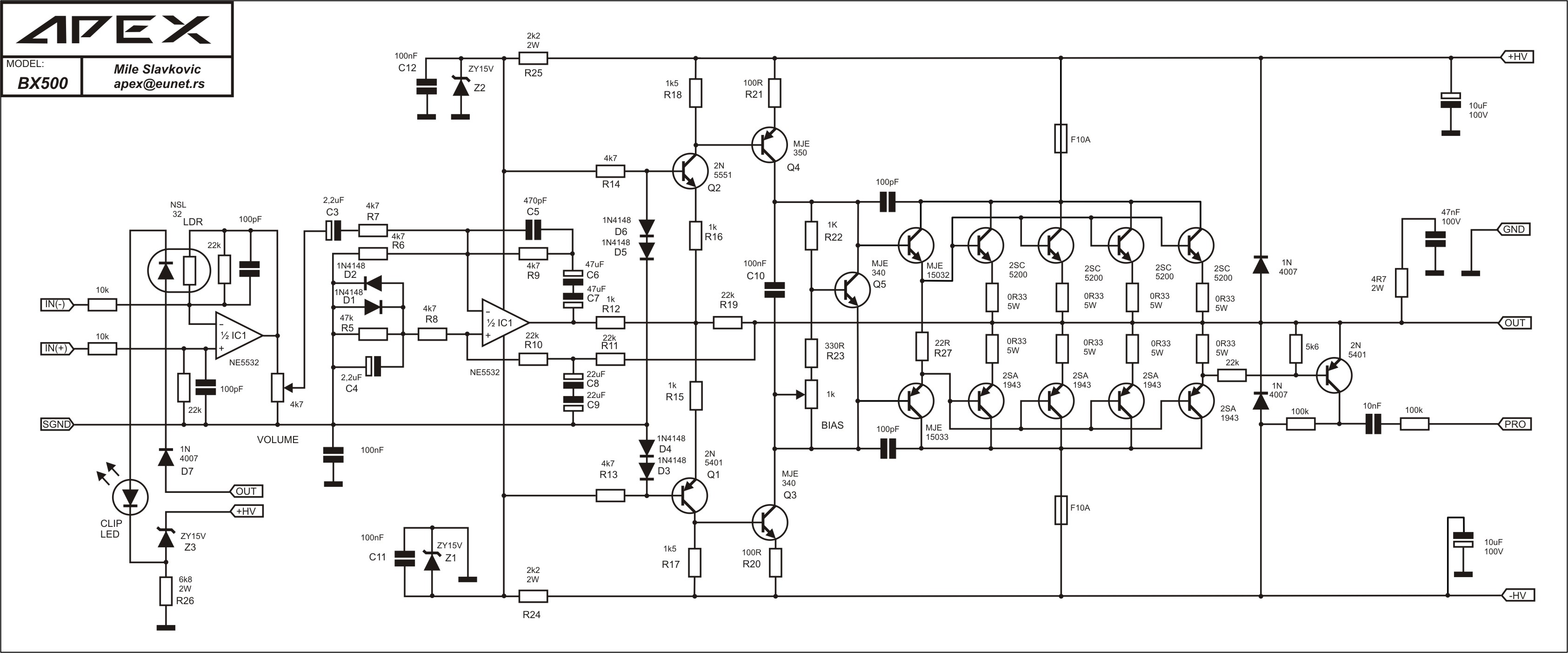

CAN YOU SEND THIS PROTECT CCT ON MY E-MAIL ptinarwo@sirdc.ac.zw i am finalising my B500 AMP. thank you
nice work sir, I am waiting for your latest PCB design for this B500
I cosidering to add signal led, fan control, VI limiter, triple darlington...
more complete and the wiring will be more modest, thank you sirI cosidering to add signal led, fan control, VI limiter, triple darlington
A little help please
Hy Apex! Please help me! I measured the amp last time before i pack it together, and one of the panels show 0.3V dc offset! The other one is fine, that is 0.2mV. How could I start to measure and where? Would it help if I post pictures?
Thanks in advance
Hy Apex! Please help me! I measured the amp last time before i pack it together, and one of the panels show 0.3V dc offset! The other one is fine, that is 0.2mV. How could I start to measure and where? Would it help if I post pictures?
Thanks in advance
Hy Apex! Please help me! I measured the amp last time before i pack it together, and one of the panels show 0.3V dc offset! The other one is fine, that is 0.2mV. How could I start to measure and where? Would it help if I post pictures?
Thanks in advance
Measure voltage on Z1, Z2 and R20, R21. Do you measure BIAS?
Measure voltage on Z1, Z2 and R20, R21. Do you measure BIAS?
Hy! I measured BIAS, it's 30-35mA in cold state for both panels. I will make the other measures as i get home from work. Do i have to measure voltage between power gnd and Z1, Z2, R20, R21?
And one more thing: I didn't connect POWER GND to SIGNAL GND, can it be the problem? But if yes, why has one of the panels 7mV DC offset (i measured it again) and the other 300mV? I can't figure it out.
Any ideas are welcome.
Measure voltage across Z1, Z2, R20, R21. Try to use mached 2N5401/5551 and MJE340/350.
urgent
for two pairs of output how many dc voltage required?
and what are the changes.
Use +/-55V rail and 1K5/2W instead 2k2/2W for R24 and R25.
Use +/-55V rail and 1K5/2W instead 2k2/2W for R24 and R25.
is it 50v dc ok for two outputs. any changes.
Use +/-55V rail and 1K5/2W instead 2k2/2W for R24 and R25.
is this correct?
Attachments
is this correct?
Yes, just 22k from overcurrent detect connect to used 0.33R/5W, +/-50V no changes for single pair.
Yes, just 22k from overcurrent detect connect to used 0.33R/5W, +/-50V no changes for single pair.
for two pair 50v dc is it ok? any changes.
Checked voltages
L Z1: 14,2V
L Z2: 14,4V
L R20: 446mV
L R21: 440mV
R Z1: 14,7V
R Z2: 14,3V
R R20: 444mV
R R21: 438mV
I used matched transistors (from the same series, and they were chosen from 15's batch with multimeter's HFE) and i used the closest possible values.
When i connect signal gnd to power gnd every reading is just fine (7-8mV offset on both panels) the 300mV offset only occours when the input pins left floating or the signal gnd is not connected to power gnd.
If it is a solution, to connect them together, then it will stay in this state.
Hello! I checked the voltages, the L and R indicates wich panel I am talking about. The R is the one with the high DC offset, the L was good so far.Measure voltage across Z1, Z2, R20, R21. Try to use mached 2N5401/5551 and MJE340/350.
L Z1: 14,2V
L Z2: 14,4V
L R20: 446mV
L R21: 440mV
R Z1: 14,7V
R Z2: 14,3V
R R20: 444mV
R R21: 438mV
I used matched transistors (from the same series, and they were chosen from 15's batch with multimeter's HFE) and i used the closest possible values.
When i connect signal gnd to power gnd every reading is just fine (7-8mV offset on both panels) the 300mV offset only occours when the input pins left floating or the signal gnd is not connected to power gnd.
If it is a solution, to connect them together, then it will stay in this state.
Hello! I checked the voltages, the L and R indicates wich panel I am talking about. The R is the one with the high DC offset, the L was good so far.
L Z1: 14,2V
L Z2: 14,4V
L R20: 446mV
L R21: 440mV
R Z1: 14,7V
R Z2: 14,3V
R R20: 444mV
R R21: 438mV
I used matched transistors (from the same series, and they were chosen from 15's batch with multimeter's HFE) and i used the closest possible values.
When i connect signal gnd to power gnd every reading is just fine (7-8mV offset on both panels) the 300mV offset only occours when the input pins left floating or the signal gnd is not connected to power gnd.
If it is a solution, to connect them together, then it will stay in this state.
Voltages are OK. Use this GND wireing if there is not hum and noise.
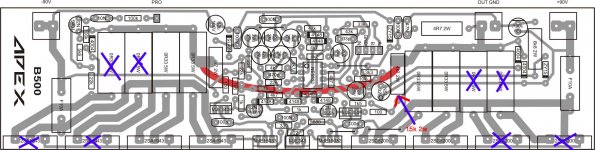
BX500 PCB design
Hi Miles....you mentioned that you were going to add these three things, are you redesigning the B500 pcb....I have added the indicator leds to my personal version of the pcb, but would like to see what your design comes out like...it is getting a bit too much for me to modify now, but I do like the XLR input stage you added a few days ago, it makes a lot of sense and actually saved me another board that had a preamp on it...less is better..still waiting to see how you will redesign the B500 to become a BX500.....I cosidering to add signal led, fan control, VI limiter, triple darlington...
Voltages are OK. Use this GND wireing if there is not hum and noise.
Thank you, i was just worried, but if you say it is ok, than i will make it this way.
Soon i will post pictures of the complete amp.
- Home
- Amplifiers
- Solid State
- 500W PA amplifier with Limiter