In my opinion, Bipolar transistors should only be used Class A.
If you go AB, D or any of them other funky letters, best abuse
some other type of device with less carrier storage weirdness.
Or drive yourself crazy making them only approximate class B,
never quite turning fully on or off. Very tricky business that....
Recovery from saturation and/or cutoff usually involves some
sort of tail spike, overshooting its way blindly out of the dark
and back into the land of analog control.
I'm going on a Rush Rampage.
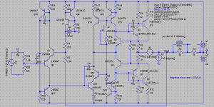
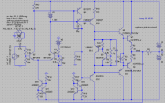
Here a version of my circuit using the Rush cascode. Distortion at 1KHz is actually better than with the LTP, but is marginally worse at 20KHz. The spectrum looks a lot better though!
The offset compensation is abused to adjust for the offset produced by the base current of the input, but the value of R3 should really be around 1.1k.
Here is the schematic.
And here is the FFT at 20KHz. This is exactly the same as what it looks like at 1KHz, just magnified by the affects of Cdom.
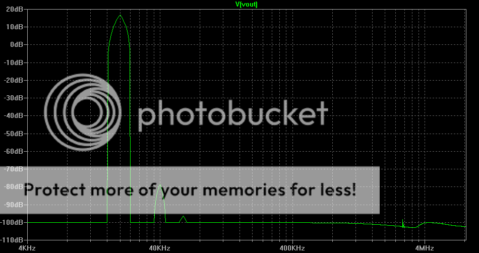
Overall, it seems the Rush Cascode has the effects of lower distortion as well as dominant 2nd harmonic, but the affect of Cdom is worse at high frequencies. If second harmonics are as pleasant as they're supposed to be, then this should not be a problem.
- keantoken
Here a version of my circuit using the Rush cascode. Distortion at 1KHz is actually better than with the LTP, but is marginally worse at 20KHz. The spectrum looks a lot better though!
The offset compensation is abused to adjust for the offset produced by the base current of the input, but the value of R3 should really be around 1.1k.
Here is the schematic.
And here is the FFT at 20KHz. This is exactly the same as what it looks like at 1KHz, just magnified by the affects of Cdom.
Overall, it seems the Rush Cascode has the effects of lower distortion as well as dominant 2nd harmonic, but the affect of Cdom is worse at high frequencies. If second harmonics are as pleasant as they're supposed to be, then this should not be a problem.
- keantoken
Member
Joined 2009
Paid Member

Thank you, Bigun. Personally, I got into class A not because of low distortion, but because it is easier. I recommend starting with class A in order to familiarize yourself with the theory without unintentional issues.
I theorize that a class-A output stage is the best to reveal the Rush Cascode's true nature...
Evil, I simulated your suggestion. I had to increase Cdom to keep it from oscillating. Seems like a good idea, but it increased THD at 20KHz. Oh, the humanity! I will have to somehow weight the benefits with the disadvantages.
- keantoken
Member
Joined 2009
Paid Member
Well, ultra-low distortion looks nice on paper, but it's not necessary, especially at 20kHz where all the harmonics are outside the range of human hearing anyway.keantoken said:...Evil, I simulated your suggestion. I had to increase Cdom to keep it from oscillating. Seems like a good idea, but it increased THD at 20KHz. Oh, the humanity! I will have to somehow weight the benefits with the disadvantages...
Another idea: You're not taking advantage of half the gain available - put the other output from the input stage to use somewhere by putting a current mirror on the collector of Q1.
kenpeter said:I don't see what keeps your DC center from drifting?
With temperature and whatnot...
Is 2SJ108 gate forward biased? If so, BJT mode now...
Nothing that would actually stop it from working....
When the temperature increases, Q4's Vbe decreases, decreasing the CCS output current. Since R2=2*R3, there is 2*Vbe(Q4) across this resistor, which compensates for the voltage drop of the two Rush transistors, which also vary with temperature. You must choose Q4 to have a tempco similar to the Rush transistors in order to have good temperature compensation.
The benefit of the Jfet is that the base current doesn't skew the output. At low currents I consider this necessary. You must know that the CCS is deliberately misadjusted to compensate for the offset created by the base current of Q2.
Bigun said:Keantoken,
Hope you don't mind, but I borrowed your spice simulation commands from post 82. They work really nicely. I'm learning everyday
I want to soon make some posts on simulation that will include the full command sets, so absolutely no problem there.
Mr Evil said:
Well, ultra-low distortion looks nice on paper, but it's not necessary, especially at 20kHz where all the harmonics are outside the range of human hearing anyway.
Another idea: You're not taking advantage of half the gain available - put the other output from the input stage to use somewhere by putting a current mirror on the collector of Q1.
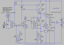
I have done this before in simulations. My modification is attached. At first I had stability problems, but the capacitors shown keep stability in check nicely it seems, with minimal rise in 20KHz distortion. Because of the voltage drop of the diode in the VAS, we have reduced VAS gain, which increases distortion to more than it was without the modifications however. I think this method is more suitable for driving a Jfet as a VAS (!).
I don't know if I remember correctly, but I think Q17 increases stability (it's probably not necessary).
Also, the feedback cap is replaced by a voltage source to keep the wandering offset from skewing the FFT.
- keantoken
Attachments
Hi keantoken,
I am following your design with some interest!
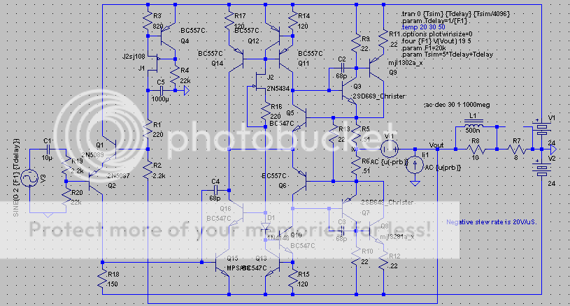
I happened to notice that your slew rate was only 20v/usec?
Wondering if there was a way to get that up to about 75v/usec?
Or, what is slowing it down...?
_-_-bear
Thank you for your interest. I hope this design might become my present listening setup soon.
If you look at the schematic in post 82, you can probably delete C2 and C3 without any adverse affects. This will help the negative slew rate (the CCS that biases the VAS will be less loaded at HF), but I don't know if the positive slew rate will improve much.
Decreasing Cdom should increase the slew rate, and I've found I can reduce Cdom lower than its present value (around 33p-47p), but I've been keeping it there to avoid any trouble in simulation.
For those of you still waiting for my post that says "yeah, I finally got it built, it sounds like blah blah blah...", it turns out I probably need new bias resistors, and the transistors I have at my bench are too fragile for this circuit. I invite anyone who wants to try it out for themselves, because it might be some time before I myself am able to do so.
Tip for stability: I was able to make the circuit stable on the bench by inserting a 33 ohm resistor between the VAS and Allison resistors (simulation show this not to affect distortion much but C2 and C3 might be needed to make it work). My breadboard setup is not very optimal, so it might not be needed for the final design.
- keantoken
keantoken said:
Tip for stability: I was able to make the circuit stable on the bench by inserting a 33 ohm resistor between the VAS and Allison resistors
- keantoken
Not resistors, transistors (oops!).
- keantoken
Here is a class AB version, just to prove I can do it.
Not sure if the temp compensation works, I don't know how to do that. But when the bias is properly adjusted, these are the simulated THD figures:
1KHz @ 30V pk-pk = .00065%
20KHz @ 30V pk-pk = .001%
1KHz @ 20V pk-pk = .00022%
20KHz @ 20V pk-pk = .00064%
Well, I've proved to myself that Class A really doesn't seem to be much better distortionwise than properly biased class AB. Don't know how it sounds.
Now if I can only build it.
P.S. How can low-distortion get any simpler than this?
- keantoken
Attachments
AndrewT said:I think the Q9 cascode desperately needs a follower to obtain low impedance drive to the two stage output EFs.
Input current to the output stage is 200uA pk-pk, more than easy for a BC557C with 6mA of bias (though I should turn up the bias a little). Maybe I'm missing something...?
I don't like the mix 33k & 3k3 for the input LTP resistances.
I don't know whether you saw this or not.
http://www.diyaudio.com/forums/showthread.php?postid=1860642#post1860642
Read to the point where MJL gets convinced, if you're that curious. Still only simulation though.
I'll play it off as "artfully asymmetric".
Why adopt a dual transistor Vbe, when most find that the single version works adequately?
I saw it in the harmon/kardon AVR35 schematic and thought it looked cool. I don't know if it's really useful, but Q5 now has constant current. I just ran a simulation and it looks like it doesn't matter. Maybe it has to do something with Q5 having more controlled Vbe/tempco characteristics, so better bias?
- keantoken
I just threw this together. This has lower impedance VAS drive. I still need a better transistor choice for the VAS follower I think.
20KHz THD @ 20v pk-pk is now .00035% (!)
1KHz THD @ 20v pk-pk is now .00014%
That was an amazing improvement.
- keantoken
20KHz THD @ 20v pk-pk is now .00035% (!)
1KHz THD @ 20v pk-pk is now .00014%
That was an amazing improvement.
- keantoken
Attachments
Okay, we must switch out Q9 Q16 Q12 and Q15 with BC556B and 546B. Performance does not suffer.
They should get hot even so... This is where my lack of experience bites me. Most people use MJE350/340 or similar in these places.
Also, the 100k resistor can be deleted.
- keantoken
They should get hot even so... This is where my lack of experience bites me. Most people use MJE350/340 or similar in these places.
Also, the 100k resistor can be deleted.
- keantoken
if you use a two stage output, driver + output, then the VAS must be a medium power device for lower impedance speakers.
If you use a three stage output, pre-driver + driver + output, then the preceeding stages can usually be To92 devices except when very low impedance loads must be driven.
Your 1302/3281 devices may be able to pass<=15Apk on very short transients.
The gain at 15Apk output is ~ 20 (>=12 in datasheet).
The peak driver current required for that 15Apk output is ~750mApk.
The gain of the 649/669 drivers at this peak current will be ~30 (datasheet shows>=30 @ 500mA)
The Driver base current from the VAS stage must be greater than 25mApk (not 0.2mA) to meet that 15Apk transient demand.
A high current To92 device can do this duty but many of it's other parameters will be compromised to achieve adequate Vce and Ic>=500mA.
You can use specialised high current To92 pre-driver (or cascode follower) to meet this duty and that then allows a fast and high gain To92 VAS to be adopted.
Reduce the peak transient output current to 5Apk, add in the quiescent currents that must flow and re-do the calculations to find the quite massive reduction in output current from the VAS. Yes, the peak transient currents really do stress the earlier stages.
- Status
- This old topic is closed. If you want to reopen this topic, contact a moderator using the "Report Post" button.
- Home
- Amplifiers
- Solid State
- 50W, Class A, another one... :)