Bridged parallel is four amplifiers. I and everyone else that understand the topology would expect 4times for the total deliverable power from four amplifiers.
National have app notes showing PA100, BA100, BPA200 and BPA300.
In each of these, each amplifier delivers within it's own rating. No magical extra power is claimed, nor is it ever created.
National have app notes showing PA100, BA100, BPA200 and BPA300.
In each of these, each amplifier delivers within it's own rating. No magical extra power is claimed, nor is it ever created.
If you go back 10, maybe 15 posts and see cucicu's chain of thought, you will see that he is not asking about bridged parallel amplifiers. He is talking about parallel bridge rectifiers. For the power supply.Bridged parallel is four amplifiers. I and everyone else that understand the topology would expect 4times for the total deliverable power from four amplifiers.
National have app notes showing PA100, BA100, BPA200 and BPA300.
In each of these, each amplifier delivers within it's own rating. No magical extra power is claimed, nor is it ever created.
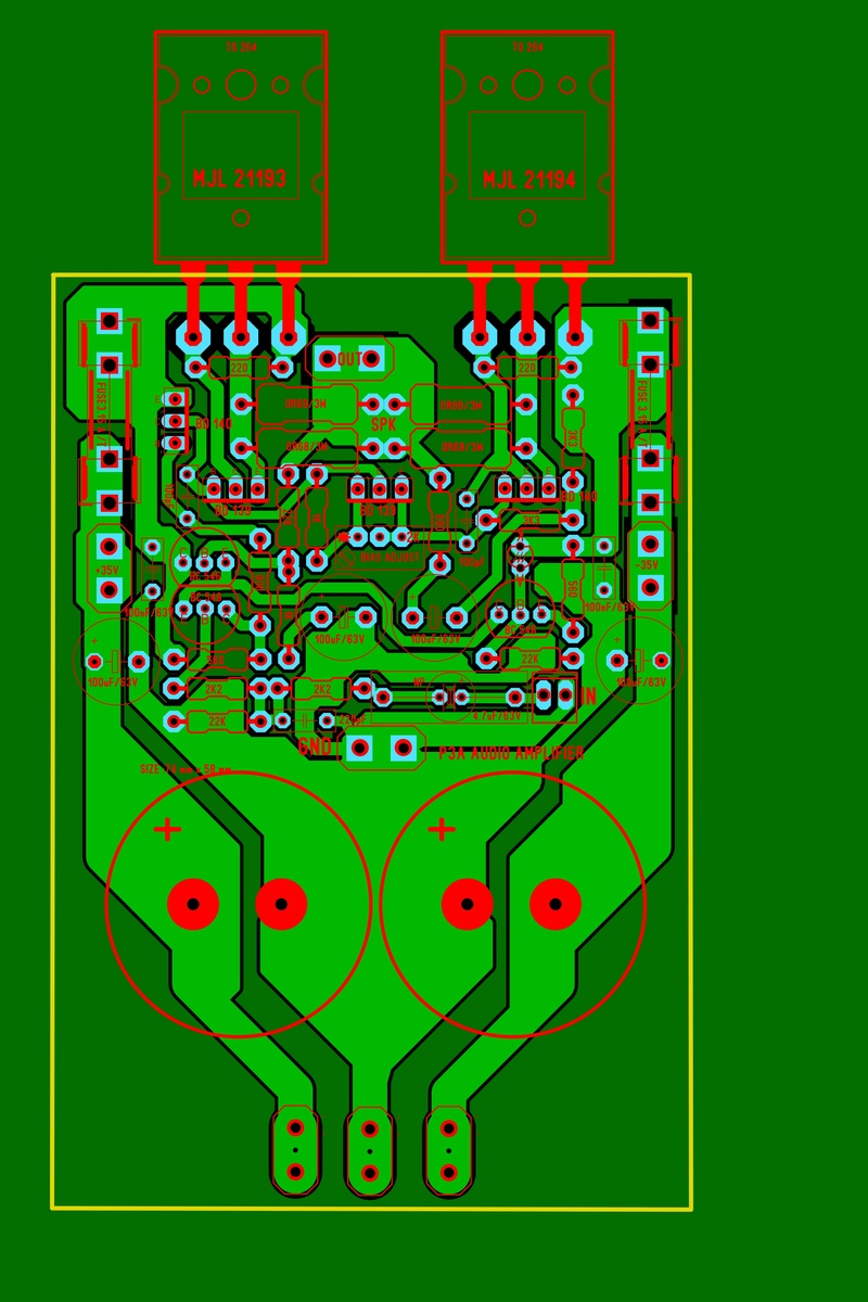
The loop area of the power input traces is far too big.
The loop area of the speaker output is far too big.
The loop area of the HF supply rail decoupling is far too big.
The Output Zobel also needs a low loop area back into the output devices and the supply rail decoupling.
The get all of these down to small loop area, the power input triplet needs to be VERY close to the output devices. Preferably between them.
The speaker output and the Power Zero Volts needs to be between the output devices as well.
Member
Joined 2009
Paid Member
Im not sure Andrew that your concerns are so serious, there are some tradeoffs to be achieved.
Id use 4 caps instead of 2, configured so you have CRC on each rail.
Id use 4 caps instead of 2, configured so you have CRC on each rail.
Last edited:
Cucicu what actually limits your design skills is cooling method think out of the box ....
On a design level size also doesn't matter make it bigger to work things around and then optimize size ...
On a design level size also doesn't matter make it bigger to work things around and then optimize size ...
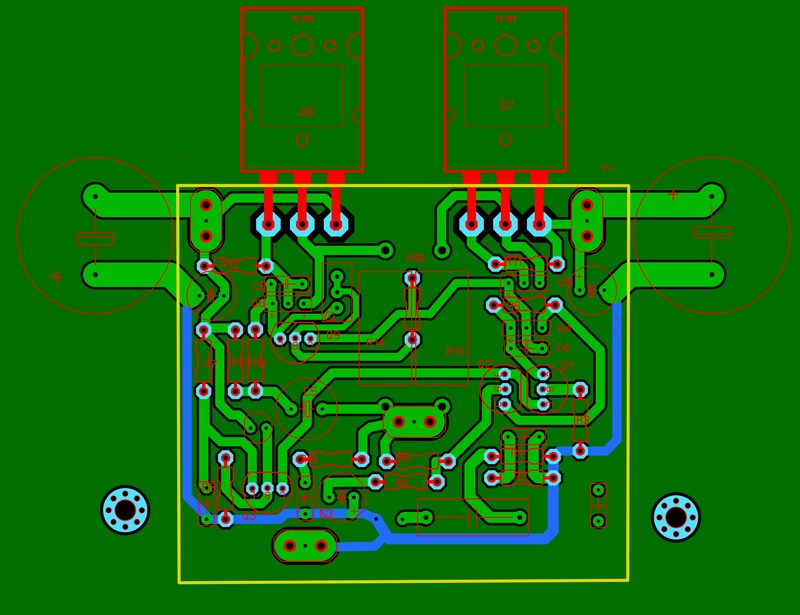
If you design wider, you can bring your power rails to the board at the top right by the output devices in the center. Put those huge caps and fuses on the supply where they belong. Bring your speaker returns to the supply, not the amp. A couple 470uF and .1uF caps will be lots at your rail feed. This will allow for really short connections from rail feed to output transistor and a twisted triplet right to the amplifier boards = less noise. Keep your input connection and input transistors as physically far away from the high power as possible with their connection traces as short as possible.
Always pay attention to current paths through capacitors. You need a distinct path for power in and power out. The above layout is a prime example of how not to connect the bulk capacitors. Power comes into the cap from the power connector, then must return through the same path to the output devices, which doubles the current flow through the trace, which causes higher resistance in the trace = less effective filtering. If the power connector and cap positions were swapped, power would run in one direction through the traces, and not have the option to bypass the filtering of the cap.
Always pay attention to current paths through capacitors. You need a distinct path for power in and power out. The above layout is a prime example of how not to connect the bulk capacitors. Power comes into the cap from the power connector, then must return through the same path to the output devices, which doubles the current flow through the trace, which causes higher resistance in the trace = less effective filtering. If the power connector and cap positions were swapped, power would run in one direction through the traces, and not have the option to bypass the filtering of the cap.
Which one would be a better option?
option1 :What if, power and gnd connector can be placed smack in between the output devices , and o/p devices can be slid further down along the PCB for so that extra space thus created between o/p device pads and PCB edge can be used to lay the ground and power trace?
option 2. 470uF caps at the sides of PCB. with adjacent power connectors, + and ground trace running along the edge of PCB to o/p device and ground trace running further to a connector placed in between the o/p devices at the top of PCB. same for - supply on the other side of PCB.
reg
Prasi
Attachments

Last edited:
I prefer to group the ground and rails close together to maintain a twisted triplet right to the board.
Yes.I prefer to group the ground and rails close together to maintain a twisted triplet right to the board.
Think how to maintain low loop area for a signal pair. Do each signal pair as a single design exercise. Then add on the next signal pair and optimise it, before moving to the third signal pair.
The power input triplet is just a conjoined pair of pairs.
I would start with the output devices at the spacing I think suits the cooling required.
Then add on the HF decoupling loop/s.
Next the MF decoupling loop/s.
Then the power triplet loop.
Then the Zobel loop
Then the speaker output loop.
When that (interference generating power current side) looks compact and buildable, you can proceed with tacking on the input signal side. Again low loop area is important. Every connection is a two wire pair that should have low loop area.
I prefer to group the ground and rails close together to maintain a twisted triplet right to the board.
Your approach is nothing more than is done by most consumer manufacturers and offers nothing more to achieve anything better to a given amplifier ...
It includes all the typical mistakes manufactures do to reduce cost
Using a triplet and include ground in the twist is screaming wrong by all means you are missing way too many things here ...
Kind regards
Sakis
PS
One should search only one post by forum member EVA which explains in a few lines what is the ideal structure for a pcb for a simple class AB amplifier regardless if this is possible to achieve or not on a single layer ....
from left to right it should be output stage power supply small signal things
It could be the other way around like psu /output stage/ small signal things
This is so easy to do only thing you need to do is redesign the cooling method ...that simple ....
many people confuse bypass and decoupling ... you can have bypass capacitors on the separated power supply if pleases you but locating banks next to the transistors , and adding 2.2uf very next to them is totaly different story and will take you to another level ....
As said a million times before the trick is that amplifier will play good enough next to many consumer amplifiers( with any of the above layouts ) and this is what makes people think that they are done with it ...In reality there is a million things to be done to make far better .
If one search which is the consumer amplifiers that created legends behind their playing performance will notice that these are the amplifiers that the designers invested not only in the schematic but also in the implementation including structure/symmetry of the pcb versus power supply .
In no case of no consumer or not amplifier you will find triplets that include ground in the twist ....
Kind regards
Sakis
Last edited:
why is the power triplet "screaming wrong"?..............
Using a triplet and include ground in the twist is screaming wrong by all means you are missing way too many things here ...
..............
Sakis, there are many thories as to how to lay out a board. Your opinion on placing caps next to the output devices has been said to cause ringing.
Your opinion on the use of grounds in the supply triplet makes no sense either. Do you care to add any sort of useful explantion as to why this is wrong.
Your opinion on the use of grounds in the supply triplet makes no sense either. Do you care to add any sort of useful explantion as to why this is wrong.
Producing a PCB for P3A more than 5 years ago ,starting from designs like the ones presented above and advancing from there while evaluating these little small details from one pcb to another which means more than 15 versions of pcb on a given design ( as was in the original circuit) took about 3 years of work and countless hours in front of a scope and a spectrum analyzer .
In most of my comments i try to give guidelines and help others to think alike but i am not willing to share for free 3 years of work ....
By the way this could be done for any given amplifier it just happened that beyond others i liked the sound of P3A as was in the first place next to many others ...
Kind regards
Sakis
- Home
- Amplifiers
- Solid State
- P3A layout