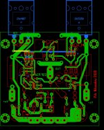
Some corrections
Wouldn't the positive and negative supply line start behaving like a dipole antenna when routed like this?
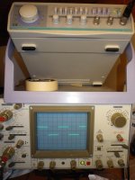
And some measurments...
1khz-square
1khz-sine clip
10khz-square
20khz square
40khz square
100khz-square
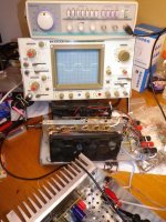
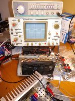
Im not finised the box yet...
I dont know ,my measurments looks good...
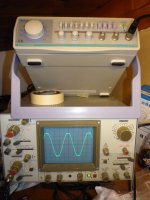
1khz-square
1khz-sine clip
10khz-square
20khz square
40khz square
100khz-square
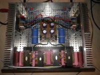
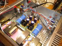
Nice build, where is the star ground and chassis connection?
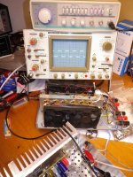
Im not finised the box yet...
Wouldn't the positive and negative supply line start behaving like a dipole antenna when routed like this?
I dont know ,my measurments looks good...
Attachments
Last edited:
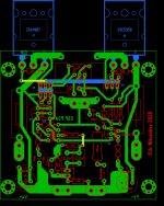
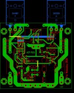
The routing of the feedback take-off point is crucial to allowing the best distortion figures. The feedback point must sample the actual loudspeaker output, using a trace carrying none of the load current. This normally means routing a trace across the loudspeaker output terminal and then on to the feedback network.
As you've drawn the layout currently the resistance of the trace between loudspeaker output and one of the emitter resistors will generate non-linear voltage directly into the feedback path. If the trace is 5 milliohms, load resistance 8 ohms, then thats ~ 600µV of error per volt of output, which is -65dB of inherent distortion (the current in each emitter resistor is mainly 2nd harmonic).
So the best layout is like:

Your latest layout still isn't combining the currents before the output terminal, its doing it on the output terminal, so it can be improved. In particular using two point connection to the spade terminal means the currents are combined on the spade terminal itself, which cannot be sampled on the PCB. Symmetry is in your favour though.
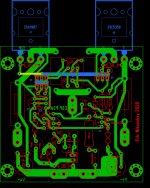
As you've drawn the layout currently the resistance of the trace between loudspeaker output and one of the emitter resistors will generate non-linear voltage directly into the feedback path. If the trace is 5 milliohms, load resistance 8 ohms, then thats ~ 600µV of error per volt of output, which is -65dB of inherent distortion (the current in each emitter resistor is mainly 2nd harmonic).
So the best layout is like:
Your latest layout still isn't combining the currents before the output terminal, its doing it on the output terminal, so it can be improved. In particular using two point connection to the spade terminal means the currents are combined on the spade terminal itself, which cannot be sampled on the PCB. Symmetry is in your favour though.
Last edited:
Well only at GHz frequencies! Magnetic interference is a near-field phenomenon, dipole antennas are far-field devices.Wouldn't the positive and negative supply line start behaving like a dipole antenna when routed like this?
Its important to keep the high current traces well away from the input section - power rails entering close to the output devices, and routed close together to cancel magnetic fields. Then the smaller supply currents feed back to the lower power parts of the circuit.
- Status
- This old topic is closed. If you want to reopen this topic, contact a moderator using the "Report Post" button.
- Home
- Amplifiers
- Solid State
- P3A layout