The same rule for Vrb for driver and pre-driver?
If pre-driver are in class A, base stopper not is necessary, it does not have a negative input impedance
Here are a few things about it:By roender- Have you ever heard about gyration theory in EF stages, where in some operating conditions every base resistance gyrate into emitter inductance? I will search trough my archive for that document...
http://www.springerlink.com/index/UPT534L357020614.pdf
By B. Cordell - Bear in mind, I am not advocating a significant reduction in bandwidth. If it is done right, there will be little reduction in speed.
As I am comparing this to my present 2 -stage T2 EF , the speed , with the same voltage amp , is far superior. The 10R collector resistors reduced my slew from 100+V/uS to the mid 80's , still WAY better than the EF I'm using now.
By raphael - This filter used R-C in Blameless-D.Self, helps prevent oscillation or is used to compensate for the deviation the filter R-C in input ?
Yes , the stability/characteristics of the voltage amp you are driving this triple with is a big factor in how stable it will be. BTW.. that filter is is NFB lead compensation , but will have little effect on local oscillations in the OPS.
By B. Cordell - We want margin. I suspect that there are many amplifiers out there where the designers struggled with the layout or whatever to stop parasitics, but had no idea how close the amplifier was to the edge, especially under different operating and load conditions. These amps can have bursts of oscillation in service that may account for poor sound that is not revealed by conventional bench testing.
Ahh , margin... the wider the better. That is what I did in simulation , brought it to the "edge" . With 3-400uH on the driver bases , one could see the bursts of oscillation while "hammering " it with square waves. Add the 10R resistors , just little highly damped bursts with a fast decay. Bring the inductances back down to something reasonable and you get perfect stability. Those larger inductances simulate a VERY craPPi layout or VERY long leads.
Another factor is the Ft of the driver /OP. For these sim's I used the 0281/0302's with a Ft of 30mhz . Funny thing is (but still predictable) , where I could simulate oscillation with these transistors , I could not with the NJW21193/4's (Ft 4mhz) .
OS
Last edited:
I put together many different triple output configuration to test for my hybrid amplifier. I never found any oscillation. The configurations (predriver/driver/output):
1, BC639/BD139/FJL4315 - BC640/BD140/FJL4215
2, KSC3503/MJE15032/FJL4315 - KSA1381/MJE15032/FJL4215
3, MJE15032/NJW0281/FJL4315 - MJE15033/NJW0302/FJL4215
4, MJE15032/NJW0281/MJL21194 - MJE15032/NJW0302/MJL21193
5, KSC2690A/MJE15032/MJL21194 - KSA1220A/MJE15033/MJL21193
6, KSC2690A/NJW0581/FJL4315 - KSC2690A/NJW0302/FJL4215
I used 4-8 pairs of out devices
Sajti
Device choice is a factor here.By sajti - I put together many different triple output configuration to test for my hybrid amplifier. I never found any oscillation. The configurations (predriver/driver/output):
Because they are so cheap here (mouser) , I have tried (or simulated) :
pre's - drivers - OP's
ksa1381/sc3503 - mje15032/33 - NJW0281/0302
ksa1381/sc3503 - NJW0281/0302 - NJW0281/0302
Ksp44/94 - mje15032/33 - NJW0281/0302
I want to try (for real)
ksa1381/sc3503 - NJW0281/0302 - NJW21193/4 (best of the choices)
or
ksa1381/sc3503 - NJW21193/4 - NJW21193/4
OS
Last edited:
KSC2690A/KSA1220A
Vce too low , I am doing 80v rails.
Still , good devices .. I use one for my LTP CCS and one for my Vbe. (ksc2690)
OS
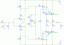
This is a kind of "triple" I`m using with no oscilation problems.
Like the "krill" (without the magic bias scheme) or the nakamitchi 620 . Did you know that the diamond itself can be the thermal comp.??
Very fast and stable.
OS
If pre-driver are in class A, base stopper not is necessary, it does not have a negative input impedance
Hi Rafael,
The pre-drivers being in class A does not change the issue with negative impedance. The pre-drivers in the Locanthi T circuit operate in class A, and yet they can, in principle, exhibit negative impedance at their bases.
Cheers,
Bob
Here are a few things about it:
http://www.springerlink.com/index/UPT534L357020614.pdf
Ahh , margin... the wider the better. That is what I did in simulation , brought it to the "edge" . With 3-400uH on the driver bases , one could see the bursts of oscillation while "hammering " it with square waves. Add the 10R resistors , just little highly damped bursts with a fast decay. Bring the inductances back down to something reasonable and you get perfect stability. Those larger inductances simulate a VERY craPPi layout or VERY long leads.
Another factor is the Ft of the driver /OP. For these sim's I used the 0281/0302's with a Ft of 30mhz . Funny thing is (but still predictable) , where I could simulate oscillation with these transistors , I could not with the NJW21193/4's (Ft 4mhz) .
OS
You are right on target.
Cheers,
Bob
The information I have is that negative impedance is due to cut-off when TRs are class B.Hi Rafael,
The pre-drivers being in class A does not change the issue with negative impedance. The pre-drivers in the Locanthi T circuit operate in class A, and yet they can, in principle, exhibit negative impedance at their bases.
Cheers,
Bob
This is a kind of "triple" I`m using with no oscilation problems.
Output bjts are Toshiba 2SC5200/SA1943.")
I tried this configuration, current required by the pre-driver (class A, opposite rails) was the same as driver....no have advantage in using
by B. Cordell - You are right on target.
Thanks , I guess that is better than missing the point.
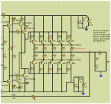
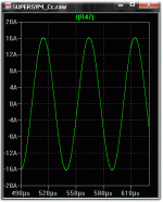
Just to "show and tell" ,and ask a few more questions I will show the final iteration of what might go to board (attachment 1).
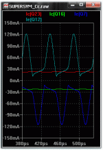
(Attachment 2) is the total current required of the drivers by 5 pair 0281/0302's (double that for the NJW21193/4's) and the CCS currents (+- 22ma). All looks good. A strange refinement occurred to me ... since the P/N devices ,while close,are not perfectly matched. This makes the crossover points slightly different (from N to P - 58ma... back from P to N 64ma , just for example.) This effect seems to happen at frequencies over 10Khz and never at 1K.
Could this be the differences in Cob/beta between the P - N devices ?? By trimming one of the driver CCS's I found I could "lock" the Xover points within a mV independent of load or freq.
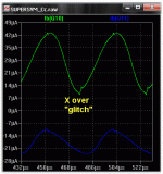
(attachment 3) This is Ib of the predrivers. With 2R loads small "glitches" occur that are perfectly in phase with the Xover points . What are they???
Any finally , the INSANE wire melting load (attachment 4) that still gives me
between .002% and .005% THD20. This holds true with either of my favorite OP's (NJW21193/4 or NJW0281/0302) , 2 - 8 R loads , and any # of OP pairs. Some might think me "thick" for wanting to keep the CCS's , but the FFT tells me to keep them as just about all the higher order harmonics are greatly reduced or eliminated. 4 more CCS led's to add to my "Xmas tree" amp ...
OS
Attachments
Last edited:
The basic cause for the impedance transform (one can look at it in either way, base-->emitter or emitter-->base) is the drop of hfe vs frequency. The critical region starts right at the point were this roll-off kicks in, if you have a transistor with hfe=100 and Ft=30MHz this point would be on the order of 300kHz, assuming a 20dB/decade rolloff.The information I have is that negative impedance is due to cut-off when TRs are class B.
This impedance transform is usually covered in modern textbooks in all detail.
Net links to a 3-part article by Dennis L.Feucht
http://www.analogzone.com/col_1017.pdf
http://www.analogzone.com/col_1121.pdf
http://www.analogzone.com/col_0116.pdf
- Klaus
Last edited:
Bob, appologies for the late reply to your resonse to my post. I will try some of your suggestions. FYI I am using 100 ohms on the pre-driver bases. I have to admit I have nobase stppers on the output devices. I use a stanars zobel (0.1 uF 400vac cap and a 3 watt low inductance resistor. I am using a 1uH L for the output inductor. The zobel is on the amplifier side of the output inductor. Just to confirm, the amp is perfectly stable until I remove the 1nf caps from the driver bases to ground.
I'll do some experimenting in the next few weeks.
Bonsai
I'll do some experimenting in the next few weeks.
Bonsai
The information I have is that negative impedance is due to cut-off when TRs are class B.
Hi Rafael,
The negative impedance seen looking into the base of an emitter follower loaded by a capacitance is due to falling AC beta of the transistor above f_beta adding another 90 degrees to the phase angle of the impedance of the capacitor, for a total of 180 degrees.
This, of course, happens in class A as well.
Cheers,
Bob
One more point that is important in regard to the use of base stopper resistors. Their use does tend to decrease thermal bias stability. This is due to the voltage drop across them that results from base current. The base stopper should usually be sized so that this voltage drop is less than 10 mV with the lowest beta expected. Less than 5 mV is even more desirable.
An output transistor biased at a current of 100 mA and with a beta of 50 will have 2 mA base current. A 5-ohm base stopper will drop 10 mV.
Cheers,
Bob
Best way I have found to aliviate this little unfortunate problem is to use a very high beta vbe multiplier transistor or even better a darlington.
by Homemodder - or even better a darlington.
I have seen this (a darlington) used by Rod elliot (esp) http://sound.westhost.com/project117.htm , on his project 117. But you say a very high beta device (such as a 2sc3503 - highest gain group Hfe 600+) would suffice ?? what device
would you suggest??
OS
- Status
- This old topic is closed. If you want to reopen this topic, contact a moderator using the "Report Post" button.
- Home
- Amplifiers
- Solid State
- Self type 3 EF (hybrid triple)... any pointers ??