I don't have the Nakamichi, i just wanted to see how similar is with the Sony CDP 750 .Sorry then, in this case only reverse enginering remains.
...By the way he also thinks it will be very hard to avoid the noise from a FPGA. The glue logic way of doing it requires only the bit clk as the highest frequency in the hole process, and that is easier to decouple than higher freqs.
Thank you for the information! However I'm not sure what you mean here. The FPGA has no clock of it's own and merely acts as a programmable set of glue logic. The only clock comes from the I2S clock.
I chose to run it this way for simplicity. Using just a low-ish jitter bit clock from something like a WM8804 or one of the various reclocking modules for CDPs without having to provide a separate clock might make it attractive to some users.
If you plan to use it for a CDP, it must be ensured that the I2S lines are at or reduced to 3.3V. It would be pertinent to check that the output isn't tied to a 5V line as well.
Last edited:
I am only referring to what I remember John said about using FPGA, so it might not be so. So you are not using the master clock , but only bit clock?.Thank you for the information! However I'm not sure what you mean here. The FPGA has no clock of it's own and merely acts as a programmable set of glue logic. The only clock comes from the I2S clock.
I chose to run it this way for simplicity. Using just a low-ish jitter bit clock from something like a WM8804 or one of the various reclocking modules for CDPs without having to provide a separate clock might make it attractive to some users.
If you plan to use it for a CDP, it must be ensured that the I2S lines are at or reduced to 3.3V. It would be pertinent to check that the output isn't tied to a 5V line as well.
As far as I can see the noise should not be worse in your implementation then.
@ecdesigns
I am planning a project with balanced signed magnitude TDA1541A.
I have a PCB from Batteryman with two TDA1541A in balanced configuration.
I was wondering if it is possible to piggyback two extra TDA1541A in such a way, that only the Data In pins are not parallel connected, but all others are so the two TDA1541A shares DEM decoupling and DEM osc. The outputs are supposed to be connected in parallel in Signed Magnitude configuration. Then I just have to connect the two top TDA1541A to the correct DATAL+/- and DATAR+/-...
No comments?@ecdesigns
I am planning a project with balanced signed magnitude TDA1541A.
I have a PCB from Batteryman with two TDA1541A in balanced configuration.
I was wondering if it is possible to piggyback two extra TDA1541A in such a way, that only the Data In pins are not parallel connected, but all others are so the two TDA1541A shares DEM decoupling and DEM osc. The outputs are supposed to be connected in parallel in Signed Magnitude configuration. Then I just have to connect the two top TDA1541A to the correct DATAL+/- and DATAR+/-...
Anybody else that have experience piggy backing TDA1541A?
Hi koldby,
In a FPGA (Field Programmable Gate Array) thousands of logic elements are capacitively coupled. When a clock signal is applied (MCK, BCK, SCK) externally it cross talks to all of these on-chip elements. We now get significant switching noise and unwanted crosstalk between elements that have different functions and should be separated for best performance. It is also not possible to apply selective decoupling (on critical parts of the circuit).
Keep the DEM clock & active divider circuits separated. The DEM clock circuit on each chip may not work reliable when paralleling the timing cap pins, using a shared timing cap.
Active dividers output a bit current. There are tolerances in bit current between chips (current reference source). When paralleling these active divider outputs you may introduce bit errors in both paralleled chips.
Also keep in mind that when you parallel active dividers, you need to double the decoupling capacitor value as the ripple current is doubled.
I was a bit hasty about the balanced version of the signed magnitude decoder. It does not work this way. When swapping DATAL+,DATAL-, DATAR+, and DATAR- you get exactly the same output signal (phase, amplitude). The only difference is that the plus halves are now processed by the other chip and vice versa.
I haven't tested this yet, but inverting DOL+, DOL-, DOR+, and DOR- for one DAC section of the balanced DAC should work.
I am only referring to what I remember John said about using FPGA, so it might not be so. So you are not using the master clock , but only bit clock?.
As far as I can see the noise should not be worse in your implementation then.
In a FPGA (Field Programmable Gate Array) thousands of logic elements are capacitively coupled. When a clock signal is applied (MCK, BCK, SCK) externally it cross talks to all of these on-chip elements. We now get significant switching noise and unwanted crosstalk between elements that have different functions and should be separated for best performance. It is also not possible to apply selective decoupling (on critical parts of the circuit).
I am planning a project with balanced signed magnitude TDA1541A.
I have a PCB from Batteryman with two TDA1541A in balanced configuration.
I was wondering if it is possible to piggyback two extra TDA1541A in such a way, that only the Data In pins are not parallel connected, but all others are so the two TDA1541A shares DEM decoupling and DEM osc. The outputs are supposed to be connected in parallel in Signed Magnitude configuration. Then I just have to connect the two top TDA1541A to the correct DATAL+/- and DATAR+/-...
Keep the DEM clock & active divider circuits separated. The DEM clock circuit on each chip may not work reliable when paralleling the timing cap pins, using a shared timing cap.
Active dividers output a bit current. There are tolerances in bit current between chips (current reference source). When paralleling these active divider outputs you may introduce bit errors in both paralleled chips.
Also keep in mind that when you parallel active dividers, you need to double the decoupling capacitor value as the ripple current is doubled.
I was a bit hasty about the balanced version of the signed magnitude decoder. It does not work this way. When swapping DATAL+,DATAL-, DATAR+, and DATAR- you get exactly the same output signal (phase, amplitude). The only difference is that the plus halves are now processed by the other chip and vice versa.
I haven't tested this yet, but inverting DOL+, DOL-, DOR+, and DOR- for one DAC section of the balanced DAC should work.
Thanks a lot for your response, John. I will find another route
and avoid piggybacking the TDA1541A.
Putting an inverter on the DOL+,DOL-, DOR+ and DOR- will probably have the same effect as doing this on a TDA1541A in normal configuration: An error on the the LSB that actually can be seen as a very small DC error until 1 LSB before digital clipping and in practice is not audible. This is the way I run my balanced TDA1541A DAC now and I only heard (and measured ) improvements as opposed to running the TDA1541A in single ended configuration.
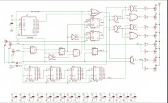
Board schematic
Here is the schematic of the board I did according to John's post Building the ultimate NOS DAC using TDA1541A
View attachment i2s-tda-nodac-v1.pdf
I changed two 74LVC1G79 D-Type flip flops to a one dual packaged 74sn74 IC hoping to have a simpler and easier to solder board. Unfortunately this is where I'm stuck at the moment. The 74sn74 IC does not seam to work as it should. I have all the signals at the inputs, but the needed Q| outputs are either static high on one flip flop output, or low on another.
Hi Sven257
In the original schematic, connect one DAC section directly to the existing non-inverted data outputs DOL+, DOL-, DOR+, DOR-
Now invert all 4 data signals (DOL+, DOL-, DOR+, DOR-) for the second section by using 74HC04, 74AHC04, 74LV04, or 74LVC04 hex inverters. Make sure to connect the inputs of the two remaining unused inverters to GND.
This way you get following 4 inverted data signals for the second DAC section:
/DOL+, /DOL-, /DOR+, /DOR-
Connect BCKO and LEO timing signals to both DAC sections.
So add 2 more 74LVC1G32 and invert the A and B inputs,
and add another 74HC08 (use 2 of 4 gates) and invert A and B inputs ??
In the original schematic, connect one DAC section directly to the existing non-inverted data outputs DOL+, DOL-, DOR+, DOR-
Now invert all 4 data signals (DOL+, DOL-, DOR+, DOR-) for the second section by using 74HC04, 74AHC04, 74LV04, or 74LVC04 hex inverters. Make sure to connect the inputs of the two remaining unused inverters to GND.
This way you get following 4 inverted data signals for the second DAC section:
/DOL+, /DOL-, /DOR+, /DOR-
Connect BCKO and LEO timing signals to both DAC sections.
SN74HC74DRHi xaled,
What is the exact type number of the dual flip-flop you used instead of the 74LVC1G80?

Hi xaled
This chip should work on 3V3 supply but depending on BCK frequency there might be a possible problem.
You could try faster logic like the 74LVC74, 74AHC74 or 74LV74 (SOIC).
When the 74xx74 receives supply voltage, 1.5 BCK delayed WS and DATA signal are within specs, and preset & clear are both connected to 3V3, these flip-flops should work.
Also consider the possibility of a solder bridge, interrupted trace or defective chip.
Hi xaled
You could try faster logic like the 74LVC74, 74AHC74 or 74LV74 (SOIC).
Will try faster ICs. Thank you for advice.
I2S to signed magnitude converter
Xaled was kind enough to send me one of his PCB he made for the I2S to Signed magnitude converter that ecdesign had developed and kindly shared with us here .
It looks like there is no problem with using the SN74HC74 Xaled had specified instead of the two LV1G80 FF from the original schematic. There is one little error (Xaled pointed that out to me ) on the PCB (U12 is missing connection to VCC) but easily corrected.
I have not yet hooked it up with the TDA1541a's, but i tested it with a 1 Hz 0dB digital signal to be able to see, what happens at the outputs.
The clk for the TDA1541A is delayed 2 bits from the falling edge of LEO and 16 bits long.
At DOL+ and DOR+ the data is only present within that window and muted half of the 1 Hz period.
At DOL- and DOR- the situation is a little different: There are data outside the window all the time, but within the window, data is muted in half of the 1 Hz period, so it will not affect the data conversion in the TDA1541A. It is a product of the way the AND/OR detector is made. My only concern is whether this unnecessary data will affect the noise situation for the TDA1541A .
I think a solution could be to add an AND gate to the DOL- and DOR- with the window signal from U17 pin4 on the other input.
Any comments from John?
Attachments
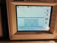
So I finally got to connect the signed magnitude converter to a TDA1541A.
I have a test DAC with Johns I2S to Simultaneous converter and a modified Red Baron TDA1541A dac. Not the same as my main dac as this is a balanced dac but again with Johns I2S to Sim. converter.
So I could just swap the I2S to Sim with I2S to Signed. and disconnect the I/U converter and connect the two outputs from the TDA1541A to each other and a 100 Ohm to GND and a 1KOhm to +5 V.
The converter did not work as planned.
I switched back to the old configuration just to be sure, but that worked perfectly.
I2S to Signed in again and here are the results:
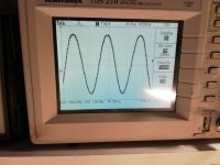
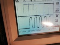
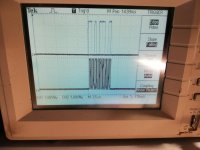
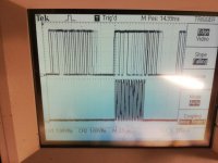
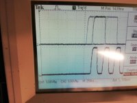
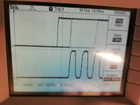
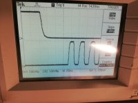
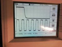
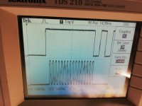
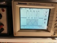
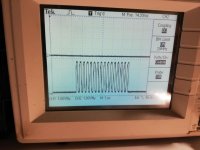
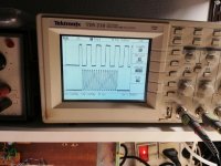
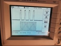
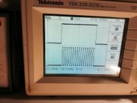
Pic. 9 shows the output with a full scale 1 Khz digital signal.
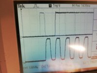
Pic. 1 shows LE and input clk
Pic. 2 shows LE and BCK01
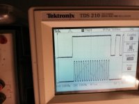
Pic. 3 shows BCK01 and DOL-
Pic. 4 shows BCK01 and DOL+
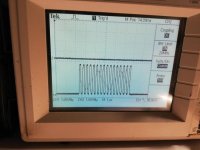
Pic. 5 and 6 shows the same with another time scale.
Pic. 7 shows BCK01 and DATAL (U14 pin 1)
Pic. 8 shows BCK01 and DATAR (u14 pin 9)
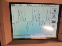
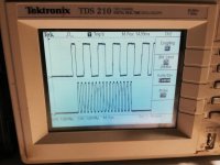
Just for fun I tried to connect DOL- and DOR+ to the DAC and to my big surprise, if I turned down one channel completely the result was as shown in Pic. 10.
If I connect DOL+ and DOR- to the DAC and only have data in the other channel it shows the same perfect result.

Now I have a headache from trying to figure out what is going on here..
Can anybody please help here???
I have a test DAC with Johns I2S to Simultaneous converter and a modified Red Baron TDA1541A dac. Not the same as my main dac as this is a balanced dac but again with Johns I2S to Sim. converter.
So I could just swap the I2S to Sim with I2S to Signed. and disconnect the I/U converter and connect the two outputs from the TDA1541A to each other and a 100 Ohm to GND and a 1KOhm to +5 V.
The converter did not work as planned.
I switched back to the old configuration just to be sure, but that worked perfectly.
I2S to Signed in again and here are the results:
Pic. 9 shows the output with a full scale 1 Khz digital signal.
Pic. 1 shows LE and input clk
Pic. 2 shows LE and BCK01
Pic. 3 shows BCK01 and DOL-
Pic. 4 shows BCK01 and DOL+
Pic. 5 and 6 shows the same with another time scale.
Pic. 7 shows BCK01 and DATAL (U14 pin 1)
Pic. 8 shows BCK01 and DATAR (u14 pin 9)
Just for fun I tried to connect DOL- and DOR+ to the DAC and to my big surprise, if I turned down one channel completely the result was as shown in Pic. 10.
If I connect DOL+ and DOR- to the DAC and only have data in the other channel it shows the same perfect result.
Now I have a headache from trying to figure out what is going on here..
Can anybody please help here???
Attachments
Xaled sent me some wav. files with artificial test signals that perhaps could say something about what is wrong.
First wav: 0101010101010101
Pic. 11 DOL-
Pic. 12 DOL+
2. Wav: 1000000000000000
Pic. 13 DOL-
Pic. 14 DOL+
3. Wav 1010101010101010
Pic. 15 DOL-
Pic. 16 DOL+
4. wav: 0111111111111111
Pic. 17 DOL-
Pic. 18 DOL+
5. wav: 1111111111111111
Pic. 19 DOL-
Pic. 20 DOL+
Actually it would have been even better if the length of the data was 17 bits and not 16 so we could see the 17. bit being clocked in to the DAC..
Attachments
- Home
- Source & Line
- Digital Line Level
- Building the ultimate NOS DAC using TDA1541A