He, he, he...you got me! 😀
This is top secret. It is not supposed to be revealed on the pick.
Better notice one of my beloved Autograph on the corner. 😎
Hey, I-m using your SPDIF CS8414 receiver for this DAC. 😉 I hope you don-t mind...
Best regards,
M
This is top secret. It is not supposed to be revealed on the pick.
Better notice one of my beloved Autograph on the corner. 😎
Hey, I-m using your SPDIF CS8414 receiver for this DAC. 😉 I hope you don-t mind...
Best regards,
M
Hi maxlorenz,
That must have been a lot of work. My compliments for successfully completing such a complicated project.
It's difficult to get a good focus on the oscilloscope screen, a tripod, or a camera with anti-shake and good auto-focus helps.
Hey John, do you want to see my modular configuration?
That must have been a lot of work. My compliments for successfully completing such a complicated project.
The picks are not so good because I had both hands on the probes
My "assistant" is an excellent (and I mean excellent) cook but a poor photographer...
It's difficult to get a good focus on the oscilloscope screen, a tripod, or a camera with anti-shake and good auto-focus helps.
Hi -EC-, 🙂
Thanks, Master...
Yeah, I prefer her as she is...
That must have been a lot of work. My compliments for successfully completing such a complicated project.
Thanks, Master...
It's difficult to get a good focus on the oscilloscope screen, a tripod with anti-shake and good auto-focus helps.
Yeah, I prefer her as she is...
Hi Art,
The charge-transfer power supply in the posted schematic is able to provide a few hundred milli-amps. It's primarily intended to power DAC chips, digital circuits, pre-amplifiers and masterclock. I used multiple charge-transfer circuits in my DI4T to spread the load current.
I suspect that the shigaclone draws too high (peak) current during power-up, resulting in a temporary voltage drop below 8V, this could prevent it from starting.
You could try shorting R4 (2.2 Ohms), this would reduce voltage drop across the charge-transfer circuit during peak currents. Other possible solution is using a transformer with a higher secondary voltage to compensate for the extra voltage drop.
It's not work. The display shown -00- but the spindle is not work. I measured 13.8V on first C and 12.8V before TeddyReg and 8.5V after TeddyReg. (Shigaclone can stand on 8-10V without problem)
The charge-transfer power supply in the posted schematic is able to provide a few hundred milli-amps. It's primarily intended to power DAC chips, digital circuits, pre-amplifiers and masterclock. I used multiple charge-transfer circuits in my DI4T to spread the load current.
I suspect that the shigaclone draws too high (peak) current during power-up, resulting in a temporary voltage drop below 8V, this could prevent it from starting.
You could try shorting R4 (2.2 Ohms), this would reduce voltage drop across the charge-transfer circuit during peak currents. Other possible solution is using a transformer with a higher secondary voltage to compensate for the extra voltage drop.
Hi Jlm0924,
The DACs have been systematically improved based on feedback during demonstrations (HiFi 2007 in Brussles, and demonstrations at Dutch audio clubs), measurements, and listening tests. I had Audiophiles and musicians come over to listen to the DAC (and the rest of the audio set), and their feedback was used to tackle specific issues. The project was started in 2006, and I have been attempting to systematically improve DAC performance ever since.
It's a basic design, I am still working on the final versions. I plan to use a fully modular configuration, using miniature modules like in post#2276.
The following modules have been designed:
- 10-bit tracker module (microcontroller-based frequency tracker for source jitter blocking).
- 12-bit tracker module (smaller, more accurate version).
- Interpolator / scrambler / WS / differential DEM clock module.
- VCXO Masterclock & clock buffer module.
- Discrete dual JFET amplifier module.
- Quad TDA1543 module with integrated I2S attenuators.
- SPDIF receiver module.
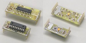
I attached a photograph of both 10-bit tracker module (large one), and the new 12-bit tracker module (small one).
The following modules still need to be designed:
- New DA1541A module.
- USB to Toslink converter module.
I am now optimizing power supplies and TDA1541A active divider decoupling caps, using an ultra-low noise 1000x pre-amp to get 1uV/div sensitivity on my oscilloscope.
Next I have to start routing the mainboards.
Hi John, I'm sure your Dac sounds great.
The DACs have been systematically improved based on feedback during demonstrations (HiFi 2007 in Brussles, and demonstrations at Dutch audio clubs), measurements, and listening tests. I had Audiophiles and musicians come over to listen to the DAC (and the rest of the audio set), and their feedback was used to tackle specific issues. The project was started in 2006, and I have been attempting to systematically improve DAC performance ever since.
It seems a couple of the experience DAC builders have built your basic design already
It's a basic design, I am still working on the final versions. I plan to use a fully modular configuration, using miniature modules like in post#2276.
The following modules have been designed:
- 10-bit tracker module (microcontroller-based frequency tracker for source jitter blocking).
- 12-bit tracker module (smaller, more accurate version).
- Interpolator / scrambler / WS / differential DEM clock module.
- VCXO Masterclock & clock buffer module.
- Discrete dual JFET amplifier module.
- Quad TDA1543 module with integrated I2S attenuators.
- SPDIF receiver module.
I attached a photograph of both 10-bit tracker module (large one), and the new 12-bit tracker module (small one).
The following modules still need to be designed:
- New DA1541A module.
- USB to Toslink converter module.
I am now optimizing power supplies and TDA1541A active divider decoupling caps, using an ultra-low noise 1000x pre-amp to get 1uV/div sensitivity on my oscilloscope.
Next I have to start routing the mainboards.
Attachments
Hi ecdesigns,
I must have missed this in the many posts in this long thread but how do you deal with the ultra-sonic out of band products that are left after the I/V conversion?
Conventional op-amp I/V designs have low pass filtering that attenuate the high frequency energy, just wondering how you get rid of it?
I must have missed this in the many posts in this long thread but how do you deal with the ultra-sonic out of band products that are left after the I/V conversion?
Conventional op-amp I/V designs have low pass filtering that attenuate the high frequency energy, just wondering how you get rid of it?
Hello
Mr Paul Tessier, in this diyaudio thread, show a merge of the digital CS8412 section of a NOS dac with the shift register part of the Cambridge DAC3 schematic, without the 7220 oversampling section.
This are doing some shift registering to give 4x oversampling. I find that this schematic could be quite easy to made.
http://www.diyaudio.com/forums/showthread.php?postid=1638842#post1638842
Anybody know if it would work correctly, without the 7220, in a non-oversampling mode, and give the correct timings/shifts and bit clock shifting result ?
Making a test board, how can we see on a scope, if, in non-os without the 7220, this schematic do give the correct timings/shifts and bit clock shifting result ?
Thank
Bye
Gaetan
Hi Rick Miller,
In standard OS DACs analogue filtering (reconstruction filters) are necessary to filter-out HF products produced by the oversampling and digital brickwall filtering process.
NOS DACs do produce significant ultra-sonic frequencies that might disrupt connected audio equipment, that's why some form of analogue (brickwall) filtering is usually required, this leads to phase errors.
If filtering is left-out completely, performance basically depends on the stability of the connected audio equipment. The ultrasonics (intermodulation with fs) usually result in distorted trebles.
DI DACs are a kind of hybrid between both OS and NOS DACs. The DI4 DACs do perform digital filtering (4x interpolator). But due to the D-I concept (using 4 D/A converters to achieve 4x interpolation), no extra noise is produced during digital filtering. Phase linearity is preserved because the filter can be compared with a simple FIR filter, these filters are phase-linear by design. The linear FIR filter, integrated in the DI4 DACs, doesn't have a brickwall filter characteristic, and it has a slow roll-off.
The 4x interpolator increases the sample rate with factor 4, so when feeding the DI4 with 44.1 KHz sample rate source, the resulting output signal sample rate will be 176.4 KHz, just like with a OS DAC running on 4x oversampling. On top of that, bit resolution is also increased (theoretically by factor 4).
The ultrasonic (out of band noise) is spread over a larger spectrum, and the average amplitude is reduced. This, and the digital filter slow roll-off will reduce out of band noise enough to leave-out analogue filters. The bandwidth of the following tube anplifier is limited , attenuating the higher frequencies (80 KHz and up). Finally the input filter in the power amplifier will further reduce HF interference that might disrupt amplifier stability.
I must have missed this in the many posts in this long thread but how do you deal with the ultra-sonic out of band products that are left after the I/V conversion?
Conventional op-amp I/V designs have low pass filtering that attenuate the high frequency energy, just wondering how you get rid of it?
In standard OS DACs analogue filtering (reconstruction filters) are necessary to filter-out HF products produced by the oversampling and digital brickwall filtering process.
NOS DACs do produce significant ultra-sonic frequencies that might disrupt connected audio equipment, that's why some form of analogue (brickwall) filtering is usually required, this leads to phase errors.
If filtering is left-out completely, performance basically depends on the stability of the connected audio equipment. The ultrasonics (intermodulation with fs) usually result in distorted trebles.
DI DACs are a kind of hybrid between both OS and NOS DACs. The DI4 DACs do perform digital filtering (4x interpolator). But due to the D-I concept (using 4 D/A converters to achieve 4x interpolation), no extra noise is produced during digital filtering. Phase linearity is preserved because the filter can be compared with a simple FIR filter, these filters are phase-linear by design. The linear FIR filter, integrated in the DI4 DACs, doesn't have a brickwall filter characteristic, and it has a slow roll-off.
The 4x interpolator increases the sample rate with factor 4, so when feeding the DI4 with 44.1 KHz sample rate source, the resulting output signal sample rate will be 176.4 KHz, just like with a OS DAC running on 4x oversampling. On top of that, bit resolution is also increased (theoretically by factor 4).
The ultrasonic (out of band noise) is spread over a larger spectrum, and the average amplitude is reduced. This, and the digital filter slow roll-off will reduce out of band noise enough to leave-out analogue filters. The bandwidth of the following tube anplifier is limited , attenuating the higher frequencies (80 KHz and up). Finally the input filter in the power amplifier will further reduce HF interference that might disrupt amplifier stability.
-ecdesigns- said:
In standard OS DACs analogue filtering (reconstruction filters) are necessary to filter-out HF products produced by the oversampling and digital brickwall filtering process.
Agreed.
-ecdesigns- said:
NOS DACs do produce significant ultra-sonic frequencies that might disrupt connected audio equipment, that's why some form of analogue (brickwall) filtering is usually required, this leads to phase errors.
I am not aware of any scientific evidence that phase errors are audible.
-ecdesigns- said:
If filtering is left-out completely, performance basically depends on the stability of the connected audio equipment. The ultrasonics (intermodulation with fs) usually result in distorted trebles.
Agreed, sounds disgusting.
-ecdesigns- said:
DI DACs are a kind of hybrid between both OS and NOS DACs. The DI4 DACs do perform digital filtering (4x interpolator).
The hardware-halfway os with linear interpolator modifies inband high frequency sines to appear as triangles on the output of the DAC.*
-ecdesigns- said:
But due to the D-I concept (using 4 D/A converters to achieve 4x interpolation), no extra noise is produced during digital filtering.
Environment friendly os, so to say.
-ecdesigns- said:
Phase linearity is preserved because the filter can be compared with a simple FIR filter, these filters are phase-linear by design. The linear FIR filter, integrated in the DI4 DACs, doesn't have a brickwall filter characteristic, and it has a slow roll-off.
And with such a slow roll-off, how does the frequency response of the DAC look like ?
-ecdesigns- said:
The 4x interpolator increases the sample rate with factor 4, so when feeding the DI4 with 44.1 KHz sample rate source, the resulting output signal sample rate will be 176.4 KHz, just like with a OS DAC running on 4x oversampling. On top of that, bit resolution is also increased (theoretically by factor 4).
Very very theoretically.
-ecdesigns- said:
The ultrasonic (out of band noise) is spread over a larger spectrum, and the average amplitude is reduced. This, and the digital filter slow roll-off will reduce out of band noise enough to leave-out analogue filters.
IYTS.
-ecdesigns- said:
The bandwidth of the following tube anplifier is limited , attenuating the higher frequencies (80 KHz and up). Finally the input filter in the power amplifier will further reduce HF interference that might disrupt amplifier stability.
Which is not really related only to this specific DAC concept.
*Which should not be regarded as a problem

Hi gaetan8888,
I assume this circuit is based on the one used in the Cambridge DAC.
It's designed for 32BCK/WS (SAA7220), meaning that when used with CS8412 (64BCK/WS), timing / interpolation will be wrong.
SAA7220, output 32BCK/WS:
0, 8, 16, and 32 BCK delays
CS8412, output 64BCK/WS,
This requires:
0, 16, 32, 48 BCK delays
Based on this, the posted circuit won't provide correct linear interpolation (wrong delay factors).
There are other "issues" with the schematic like cascading 3 x LS04 buffers to drive the DAC chips. Driving 4 DAC chips with only 1 "clock buffer", failing to provide the absolutely required synchronization of the DEM clocks when using multiple TDA1541A chips, and running the CS8412 in master mode (very high jitter).
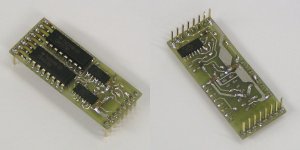
I recently posted a complete miniature interpolator module (only 5 ICs) that CAN be used with SPDIF receivers like the CS8412. I used 2 * twin-64-bit shift-register with taps on 16, 32, 48, and 64. It providing 4 x 64-bit shift-registers. In addition to the 4x linear interpolator, it also has an integrated scrambler that compensates for stereo DAC on-chip L/R channel tolerances, integrated divider that outputs WS (BCK/64)for slaving a SPDIF receiver, and a differential 352.8 KHz DEM clock output (BCK/8) for the latest synchronous DEM clock circuit. All DATA and WS outputs have resistors installed that are part of the I2S attenuators.
The module has 16 pins:
WS16, WS32, WS48, WS64, D16(L/R), ND48(NR/NL), D32(L/R), ND64(NR/NL), VCC, BCK-in, WS-out, NDEM, DEM, DATA in, GND(2x).
I used the available DLY16 outputs to drive the first DAC (similar function as the 2 D-flip flops in the posted schematic), this results in adding 16 to the other 3 delayed outputs.
Anybody know if it would work correctly, without the 7220, in a non-oversampling mode, and give the correct timings/shifts and bit clock shifting result ?
I assume this circuit is based on the one used in the Cambridge DAC.
It's designed for 32BCK/WS (SAA7220), meaning that when used with CS8412 (64BCK/WS), timing / interpolation will be wrong.
SAA7220, output 32BCK/WS:
0, 8, 16, and 32 BCK delays
CS8412, output 64BCK/WS,
This requires:
0, 16, 32, 48 BCK delays
Based on this, the posted circuit won't provide correct linear interpolation (wrong delay factors).
There are other "issues" with the schematic like cascading 3 x LS04 buffers to drive the DAC chips. Driving 4 DAC chips with only 1 "clock buffer", failing to provide the absolutely required synchronization of the DEM clocks when using multiple TDA1541A chips, and running the CS8412 in master mode (very high jitter).
I recently posted a complete miniature interpolator module (only 5 ICs) that CAN be used with SPDIF receivers like the CS8412. I used 2 * twin-64-bit shift-register with taps on 16, 32, 48, and 64. It providing 4 x 64-bit shift-registers. In addition to the 4x linear interpolator, it also has an integrated scrambler that compensates for stereo DAC on-chip L/R channel tolerances, integrated divider that outputs WS (BCK/64)for slaving a SPDIF receiver, and a differential 352.8 KHz DEM clock output (BCK/8) for the latest synchronous DEM clock circuit. All DATA and WS outputs have resistors installed that are part of the I2S attenuators.
The module has 16 pins:
WS16, WS32, WS48, WS64, D16(L/R), ND48(NR/NL), D32(L/R), ND64(NR/NL), VCC, BCK-in, WS-out, NDEM, DEM, DATA in, GND(2x).
I used the available DLY16 outputs to drive the first DAC (similar function as the 2 D-flip flops in the posted schematic), this results in adding 16 to the other 3 delayed outputs.
Attachments
Hi ecdesigns,
Thanks for the explanation of how your DAC works. I was not aware that your digital filters slow roll off plus the filters in your tube stage and power amp provided enough rejection of the ultra-sonic energy. I assume that the filters in the tube stage and power amp are first order 6db/octave filters that are -3db around 80Khz.
I am using a Phillips CD-40 with at I/V stage like the one Walt Jung wrote up in the US magazine “The Audio Amateur” issue two ’92 page 16. It uses a three-pole Bessel filter with Analog Devices AD811 current feedback amplifiers.
I would like to try your passive I/V approach but I don’t think it would work with the single TDA1541 in my CD-40.
-ecdesigns- said:Hi gaetan8888,
...
I recently posted a complete miniature interpolator module (only 5 ICs) that CAN be used with SPDIF receivers like the CS8412. I used 2 * twin-64-bit shift-register with taps on 16, 32, 48, and 64. It providing 4 x 64-bit shift-registers. In addition to the 4x linear interpolator, it also has an integrated scrambler that compensates for stereo DAC on-chip L/R channel tolerances, integrated divider that outputs WS (BCK/64)for slaving a SPDIF receiver, and a differential 352.8 KHz DEM clock output (BCK/8) for the latest synchronous DEM clock circuit. All DATA and WS outputs have resistors installed that are part of the I2S attenuators.
The module has 16 pins:
WS16, WS32, WS48, WS64, D16(L/R), ND48(NR/NL), D32(L/R), ND64(NR/NL), VCC, BCK-in, WS-out, NDEM, DEM, DATA in, GND(2x).
I used the available DLY16 outputs to drive the first DAC (similar function as the 2 D-flip flops in the posted schematic), this results in adding 16 to the other 3 delayed outputs.
Hello
I presume this module are the DI4 dac, but it seem a bit complicated for me, do you have a schematic of your DI4 dac ?
Thank a lot for your explanations.
Gaetan
Hi John,
I wonder if the DI design could be implemented with 4x pcm1704 per channel achieving 8x sampling rate interpolation.
I wonder if the DI design could be implemented with 4x pcm1704 per channel achieving 8x sampling rate interpolation.
Hi Bernhardt,
Actually, DI16 output was a perfect sine at 20Khz. DI4M output looks like a Mayan (stepped) pyramid to me, at 20Khz...yet DI4M sounds MUCH cleaner, detailed and extended on the sweet highs.
Cheers,
M
PS: I did some extensive listening to my DI4M yesterday ( not comparing to the DI4 without scrambler face to face yet) and it sounded way better tan my TeddyRegged M-Audio superDAC (AK4393; fed with Monarchy Audio upsampler) which wears unfortunately an aggressive first order filter that I have to tweak.
quote: Originally posted by -ecdesigns- DI DACs are a kind of hybrid between both OS and NOS DACs. The DI4 DACs do perform digital filtering (4x interpolator).
->The hardware-halfway os with linear interpolator modifies inband high frequency sines to appear as triangles on the output of the DAC.*
*Which should not be regarded as a problem...
Actually, DI16 output was a perfect sine at 20Khz. DI4M output looks like a Mayan (stepped) pyramid to me, at 20Khz...yet DI4M sounds MUCH cleaner, detailed and extended on the sweet highs.
Cheers,
M
PS: I did some extensive listening to my DI4M yesterday ( not comparing to the DI4 without scrambler face to face yet) and it sounded way better tan my TeddyRegged M-Audio superDAC (AK4393; fed with Monarchy Audio upsampler) which wears unfortunately an aggressive first order filter that I have to tweak.
Charge transfer PS
Dear John,
I am now enjoying my first PS with the charge transfer concept on the digital section of my DI4(1). It works evidently!
Sound is more liquid, and authoritative yet more transparent.
I am going to start buying MOSFETs as a madman 😀
and put the circuit everywhere!
I think my Class D amps would benefit from this also.
You did it again 🙂
Thanks a lot.
M
Thanks to John and Max. I'll try as you suggest and keep report back to you next year.
Happy new year to you all.
Regards,
Art.
Happy new year to you all.
Regards,
Art.
hi
I'm a beginner from china and poor english.
can someone tell me how to build DI16 with TDA1545A?
I'm a beginner from china and poor english.
can someone tell me how to build DI16 with TDA1545A?
Sam27 you may be SOL.
I don't think this is a project for beginners even for Engish speaking ones. I would suggest you get help from an experienced DIY builder.
I don't think this is a project for beginners even for Engish speaking ones. I would suggest you get help from an experienced DIY builder.
Hi Telstar,
Interpolation needs to be identical for both channels, so with 4 x mono PCM1704 for each channel, only 4 x DI can be achieved.
The PCM1704 interface is also different from the TDA154X, and it's a mono DAC, this requires a complete re-design of the existing DI / scrambler circuit.
I wonder if the DI design could be implemented with 4x pcm1704 per channel achieving 8x sampling rate interpolation.
Interpolation needs to be identical for both channels, so with 4 x mono PCM1704 for each channel, only 4 x DI can be achieved.
The PCM1704 interface is also different from the TDA154X, and it's a mono DAC, this requires a complete re-design of the existing DI / scrambler circuit.
-ecdesigns- said:this requires a complete re-design of the existing DI / scrambler circuit.
Knowing you, it will be ready, let say mid January? 😉
Thanks for all the interesting ideas and info you shared John. Very much appreciated and I wish you a productive 2009 with even more ideas to share
May be Vacation this year? 😀
- Home
- Source & Line
- Digital Line Level
- Building the ultimate NOS DAC using TDA1541A