Hi Erik,
What's the point of seeking more opinions. The wonder
of this forum is that we have truly great enthusiast like EC who's
willing to share his knowledge & experience with us. All it takes
is to build it ourselves & experience it. It does'nt cost a bomb for the parts. Besides after building, we can discuss our success or
failure in this forum.
Opinions will always vary just like food. Everyone has different
likings.
Hi ErikdeBest,
I read the reaction of smoking amp (Don),
The charge-transfer power supply prevents a direct charge current path between both transformer and all connected loads, bypass caps, and wiring. Filters won't.
The output ripple voltage of the charge-transfer power supply is typical 3 times lower than the ripple voltage on the primary cap. Typical values:
Primary cap ripple voltage, 600mV rms, charge-transfer circuit output, 200mV rms.
The charge-transfer current is already limited by a 2.2 Ohm drain series resistor.Today I optimized transfer current characteristics by using a modified gate drive circuit.
The charge-transfer power supply is followed by a capacitance multiplier that reduces the 200mV rms ripple to values below approx. 100uV rms.
This voltage is then fed to an ultra low noise voltage regulator (2 ... 260nV root Hz).
The noise that manages to pass these 3 cascaded circuits will be filtered-out by using passive filters.
I wouldn't have developed a "nutty" charge-transfer power supply if I could match, or outperform a battery power supply by just using a conventional power supply with (passive) filters.
The charge-transfer power supply seems like a fantastic implementation. Enthousiastac as I am I just posted your explanation on the charge-transfer power supply in the tubes forum, to see what people over there think about it.
I read the reaction of smoking amp (Don),
It is far safer to just use proper filtering to get rid of the HF line noise than such a nutty switching approach
The charge-transfer power supply prevents a direct charge current path between both transformer and all connected loads, bypass caps, and wiring. Filters won't.
The output ripple voltage of the charge-transfer power supply is typical 3 times lower than the ripple voltage on the primary cap. Typical values:
Primary cap ripple voltage, 600mV rms, charge-transfer circuit output, 200mV rms.
The charge-transfer current is already limited by a 2.2 Ohm drain series resistor.Today I optimized transfer current characteristics by using a modified gate drive circuit.
The charge-transfer power supply is followed by a capacitance multiplier that reduces the 200mV rms ripple to values below approx. 100uV rms.
This voltage is then fed to an ultra low noise voltage regulator (2 ... 260nV root Hz).
The noise that manages to pass these 3 cascaded circuits will be filtered-out by using passive filters.
I wouldn't have developed a "nutty" charge-transfer power supply if I could match, or outperform a battery power supply by just using a conventional power supply with (passive) filters.
The charge-transfer power supply is followed by a capacitance multiplier that reduces the 200mV rms ripple to values below approx. 100uV rms.
This voltage is then fed to an ultra low noise voltage regulator (2 ... 260nV root
Do you think it is possible to use a LCLCL filter to replace the capacitance multiplier and voltage regulator, at least for your tube amplifier B+?
I am just wondering what the results will be.
Hi PyroVeso,
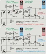
I attached the schematics of the charge-transfer power supplies that are being tested in the DI4T. There are two versions, one for a positive power supply, and one for a negative power supply.
Both D1 and D2 are rectifier diodes, D3 is added for generating a 100 / 120 Hz pulsed-DC signal for driving the gate of T1. D1 ... D3 are Schottky diodes.
R1 limits the current through the MOSFET internal gate protection diodes. If a MOSFET is selected that hasn't got internal gate protection diodes, these have to be added externally (2 x 12V zener with cathodes connected together, connected between both gate and source).
R2 (1 M Ohm) forms an LC filter together with the approx. 1.1nF gate capacitance, this will reduce the peak charge-transfer current when the MOSFET switches-ON. D5 (Schottky diode) ensures rapid switch-off by bypassing R2 during switching-OFF the MOSFET T1. The MOSFETs aren't critical, but should be suitable to handle required current and voltage, low RDSon is preferred.
D4 is added because the 2SJ380 has an internal freewheeling diode between both source and drain, it also reduces the effect of both MOSFET output and transfer capacitance. R4 limits the peak charge current during charge-transfer between C1 and C2. R3 is required to pull the gate of T1 to ground when D1 ... D3 no longer conduct.
T2 forms a capacitance multiplier, it's basically a source follower that buffers the voltage across C3. The advantage of using a MOSFET is higher efficiency than when using darlingtons, especially with higher output currents. It's best to use logic level MOSFETs here (lowest voltage drop), typical voltage drop is between approx. 1.6 ... 2V. Both charge-transfer circuit and gyrator will introduce a typical voltage drop of approx. 4 volts.
Both C1 and C2 value depend on required load current. The indicated values are for approx. 250mA.
It's also possible to use half-wave rectification, then D2, D3, and R3 are left-out. R1 goes to the anode of D1, and R2 is increased to approx. 3.3 M Ohm.
The charge-transfer power supply output is connected to a suitable voltage regulator that basically receives a clean DC input voltage without significant ripple voltage.
When building High-Voltage versions for a tube power supply, High-voltage fast-slow recovery diodes have to be placed in series with D1 ... D4. The voltage rating of both capacitors and MOSFETs must be adapted to the required voltage and load current. I use 2 x 68uF/400V for the DI4T tube power supply.
The values of resistors 1 ... 4 needs to be adapted too, for example R1 = 470K, R2 = 4M7, R3 = 100K, R4 = 22R (depends on MOSFET specifications).
The circuit could be further optimized by providing a constant charge-transfer current (current regulator).
Could you please post the last optimized schematics of the charge-transfer power supply + capacitance multiplier + ultra low noise voltage regulator? I want to experiment with these circuits right now.
I attached the schematics of the charge-transfer power supplies that are being tested in the DI4T. There are two versions, one for a positive power supply, and one for a negative power supply.
Both D1 and D2 are rectifier diodes, D3 is added for generating a 100 / 120 Hz pulsed-DC signal for driving the gate of T1. D1 ... D3 are Schottky diodes.
R1 limits the current through the MOSFET internal gate protection diodes. If a MOSFET is selected that hasn't got internal gate protection diodes, these have to be added externally (2 x 12V zener with cathodes connected together, connected between both gate and source).
R2 (1 M Ohm) forms an LC filter together with the approx. 1.1nF gate capacitance, this will reduce the peak charge-transfer current when the MOSFET switches-ON. D5 (Schottky diode) ensures rapid switch-off by bypassing R2 during switching-OFF the MOSFET T1. The MOSFETs aren't critical, but should be suitable to handle required current and voltage, low RDSon is preferred.
D4 is added because the 2SJ380 has an internal freewheeling diode between both source and drain, it also reduces the effect of both MOSFET output and transfer capacitance. R4 limits the peak charge current during charge-transfer between C1 and C2. R3 is required to pull the gate of T1 to ground when D1 ... D3 no longer conduct.
T2 forms a capacitance multiplier, it's basically a source follower that buffers the voltage across C3. The advantage of using a MOSFET is higher efficiency than when using darlingtons, especially with higher output currents. It's best to use logic level MOSFETs here (lowest voltage drop), typical voltage drop is between approx. 1.6 ... 2V. Both charge-transfer circuit and gyrator will introduce a typical voltage drop of approx. 4 volts.
Both C1 and C2 value depend on required load current. The indicated values are for approx. 250mA.
It's also possible to use half-wave rectification, then D2, D3, and R3 are left-out. R1 goes to the anode of D1, and R2 is increased to approx. 3.3 M Ohm.
The charge-transfer power supply output is connected to a suitable voltage regulator that basically receives a clean DC input voltage without significant ripple voltage.
When building High-Voltage versions for a tube power supply, High-voltage fast-slow recovery diodes have to be placed in series with D1 ... D4. The voltage rating of both capacitors and MOSFETs must be adapted to the required voltage and load current. I use 2 x 68uF/400V for the DI4T tube power supply.
The values of resistors 1 ... 4 needs to be adapted too, for example R1 = 470K, R2 = 4M7, R3 = 100K, R4 = 22R (depends on MOSFET specifications).
The circuit could be further optimized by providing a constant charge-transfer current (current regulator).
Attachments
Hi agent.5,
The capacitance multiplier is required to achieve very low ripple voltages on B+ (typical < 100uV rms). It's a very compact and cheap circuit compared to multiple chokes and electrolytic capacitors.
Voltage regulator is preferred (stable voltage). LC filters can be added after the voltage regulator to get rid of residual RF / HF noise.
I already use small LC filters (20 Henry and 47uF), after the HV charge-transfer transfer power supply, capacitance multiplier, and voltage regulator.
Do you think it is possible to use a LCLCL filter to replace the capacitance multiplier and voltage regulator, at least for your tube amplifier B+?
The capacitance multiplier is required to achieve very low ripple voltages on B+ (typical < 100uV rms). It's a very compact and cheap circuit compared to multiple chokes and electrolytic capacitors.
Voltage regulator is preferred (stable voltage). LC filters can be added after the voltage regulator to get rid of residual RF / HF noise.
I already use small LC filters (20 Henry and 47uF), after the HV charge-transfer transfer power supply, capacitance multiplier, and voltage regulator.
Hi -EC-. Thanks for your altruism. ")
What about Mosfet's VGS(th)?
The gyrator, as said by the guys who developed the TeddyReg, "sound" different depending on the active device used and the quality of C and R.
That is true for analog circuits. I don't know how could this affect digital circuits...
Cheers,
M
What about Mosfet's VGS(th)?
The gyrator, as said by the guys who developed the TeddyReg, "sound" different depending on the active device used and the quality of C and R.
That is true for analog circuits. I don't know how could this affect digital circuits...
Cheers,
M
Hi JC951t,
The charge-transfer power supply can be used with both single and twin secondary transformer windings. It can also be used with either half (50 / 60 Hz) or full wave (100 / 120 Hz) rectifiers.
Example:
Single secondary winding > plus and minus supply > half-wave > 50 / 60 Hz
Single secondary winding > plus or minus supply > full-wave > 100 / 120 Hz (using bridge rectifier)
Dual secondary windings > plus and minus supply > full-wave > 100 / 120 Hz (using bridge rectifier)
Dual secondary windings > dual plus and dual minus supply > half-wave > 50 / 60 Hz
Keep in mind that every transformer has a capacitance between both primary and secondary windings (can be checked with capacitance meter), it's usually a few hundred pF and varies with both transformer type and size. This capacitance is basically connected between both mains and secondary circuits.
The more (bigger) transformers used in a circuit, the higher the cumulated capacitance.
Since the charge transfer circuit requires a CT trans, is
it wise to power a positive & negative circuit using 1
trans ?
The charge-transfer power supply can be used with both single and twin secondary transformer windings. It can also be used with either half (50 / 60 Hz) or full wave (100 / 120 Hz) rectifiers.
Example:
Single secondary winding > plus and minus supply > half-wave > 50 / 60 Hz
Single secondary winding > plus or minus supply > full-wave > 100 / 120 Hz (using bridge rectifier)
Dual secondary windings > plus and minus supply > full-wave > 100 / 120 Hz (using bridge rectifier)
Dual secondary windings > dual plus and dual minus supply > half-wave > 50 / 60 Hz
Keep in mind that every transformer has a capacitance between both primary and secondary windings (can be checked with capacitance meter), it's usually a few hundred pF and varies with both transformer type and size. This capacitance is basically connected between both mains and secondary circuits.
The more (bigger) transformers used in a circuit, the higher the cumulated capacitance.
Hi maxlorenz,
The MOSFET gate threshold voltage is not very important for the charge-transfer circuit (plenty of voltage to drive the gate).
With the capacitance multiplier, Vgs(th) is rather important, as it directly translates to the voltage drop (efficiency) across the circuit. So here MOSFETS with lower Vgs(th), usually called logic level MOSFETS are preferred.
The Teddyreg output voltage varies with load current, this may result in load-dependent interactions (ripple / noise). This in turn may translate to different perceived sound quality. By using components with different properties, the interactions could be different, this may lead to a different interference harmonics pattern, affecting the connected circuits in a different way.
One of many effects on digital circuits could be both increased timing jitter, and different jitter spectrum.
What about Mosfet's VGS(th)?
The MOSFET gate threshold voltage is not very important for the charge-transfer circuit (plenty of voltage to drive the gate).
With the capacitance multiplier, Vgs(th) is rather important, as it directly translates to the voltage drop (efficiency) across the circuit. So here MOSFETS with lower Vgs(th), usually called logic level MOSFETS are preferred.
The gyrator, as said by the guys who developed the TeddyReg, "sound" different depending on the active device used and the quality of C and R.
That is true for analog circuits. I don't know how could this affect digital circuits...
The Teddyreg output voltage varies with load current, this may result in load-dependent interactions (ripple / noise). This in turn may translate to different perceived sound quality. By using components with different properties, the interactions could be different, this may lead to a different interference harmonics pattern, affecting the connected circuits in a different way.
One of many effects on digital circuits could be both increased timing jitter, and different jitter spectrum.
Hi ecdesigns,
Have you ever thought about using bipolar transistors for the switch and cap multiplier? I have found that low capacitance parts like the D44 & D45 series of bipolars work very well for low C series pass devices. I use the D44VH10 and D45VH10 in my power supplies. For a series pass device I have not found anything better, for low C and high Ft bandwidth. They really help keep RFI from passing thru to the active circuitry.
Rick
Hi John (-ecdesigns-),
Because 2SK2391 is rather obsolete part, could we use 2SK2232 instead? (it is a bit faster, Vds = 60V, Rds(on) = 0.036 Ohm, Vth = 0.8 - 2 V, with a bit bigger in/out capacitance)
Also appropriate could be IRL540N (recommended by Farnell as a replacement of 2SK2391), IRL530N (I think - with nearer parameters), NTE2396 (recommended by Toshiba as a replacement).
Hi John, colleagues
I was away for two days and now I see some reactions that make me think that I acted in a way as not trusting John's work, and therefore I have to question it in another forum. Well, that wasn't the intention... I posted the "charge-transfer power supply" in the tubes forum as I like the guys over there and thought they could use it as well. I could as well have posted it in the pass forum, or in the PS forum....
It may have sounded so, but it was by no means intended to question John's circuit. I am also not discouraged by the comments of Don (smoking-amp) and I will try it - for sure. As commented here, the components are cheap and the circuit is easy to put together...still my projects run a 100x slower than John's and I have some other things to conclude first.
I already was at John's place to listen to the early DI-8 DAC...I almost bought the PCB's, but when I had the money together John came with the improved DI-4M and now I am saving money to get these boards instead.
Erik
Hi Erik,
Looks like your good intentions have gone
to waste. Maybe it's cultural. I'm a Chinese.
In our culture it is taboo. Meaning, that you
do not respect a person in this case it is
John. Anyway as in anything in life, theres
always a difference of opinion. Best thing to
do is to try things out & decide for ourselves.
Cheers
HI JC951t
Well, at least you understood that it was originally meant as a good intention. But, well, ya know, the world is full of them, ain't it? and everybody has a different opinion on what a good intention is...
Sure it is a cultural issue... and having acquired some experience with Dutch culture (I am in fact Brazilian) I think that who is less bothered with this issue is John himself. It is just my Brazilian culture that push me to set things straight se we can all go through the same door at the end of the day (though that is in fact a Dutch expression).
Erik
Hi John
You already described the modifications needed for a HV version, but I just want to confirm two small things:
1 - About the HV diode in serie with the Schottky. Is this the same as the hybrid version as described in post #2110?
Is any form of voltage equalization needed across these diodes?
2 - About D5. Will the BAT42 survive the high voltage circuit? This is just a demonstration that in fact I do not know everything what is going on there. I do think that the voltage between source and gate will never exceed the maximum voltage of the BAT42, but I would like to ask anyway.
I found two high voltage P-channel mosfets: the MTP2P50E by ONSEMI and the FQP3P50 by FAIRCHILD. Both will require the addition of the 2 12V zeners. Do you have another suggestion for a HV mosfet?
Many thanks, Erik
You already described the modifications needed for a HV version, but I just want to confirm two small things:
1 - About the HV diode in serie with the Schottky. Is this the same as the hybrid version as described in post #2110?
I also used Schottky 1.1KV / 1A Hybrid diodes in the HV tube power supply. These provide a very clean sound, I tested these diodes with a pulse generator, recovery is identical to Schottky diodes.
Is any form of voltage equalization needed across these diodes?
2 - About D5. Will the BAT42 survive the high voltage circuit? This is just a demonstration that in fact I do not know everything what is going on there. I do think that the voltage between source and gate will never exceed the maximum voltage of the BAT42, but I would like to ask anyway.
I found two high voltage P-channel mosfets: the MTP2P50E by ONSEMI and the FQP3P50 by FAIRCHILD. Both will require the addition of the 2 12V zeners. Do you have another suggestion for a HV mosfet?
Many thanks, Erik
- Home
- Source & Line
- Digital Line Level
- Building the ultimate NOS DAC using TDA1541A