Finally got the TPA3250D2 card layout done. Decided to keep the Wiener theme going with the board naming, the card's now called the Wiener Pro. The layout is just as OCD as the TPA3118 Wiener card 😉
For some reason the drill holes aren't showing up with this gerber viewer, but they're there.

Schematic is similar to what I posted earlier, but with the input diode clamps and gain selection jumpers hauled out. PCB size is 11x7cm, inductors are now ICE Components 1D17A instead of the original Coilcrafts. I've got a couple spots for through-hole 1/4W resistors on the input side, installing resistors will increase the gain. I'll configure the board for 20dB by default and throw in resistors for 26 and 32dB.
When I order boards for the next Wiener group buy in the coming weeks, I'll order boards/parts and build one up to try.
For some reason the drill holes aren't showing up with this gerber viewer, but they're there.
Schematic is similar to what I posted earlier, but with the input diode clamps and gain selection jumpers hauled out. PCB size is 11x7cm, inductors are now ICE Components 1D17A instead of the original Coilcrafts. I've got a couple spots for through-hole 1/4W resistors on the input side, installing resistors will increase the gain. I'll configure the board for 20dB by default and throw in resistors for 26 and 32dB.
When I order boards for the next Wiener group buy in the coming weeks, I'll order boards/parts and build one up to try.
Is there any reason to upgrade from TPA3118 to TPA3251 (let's say from the Wiener to the Wiener Pro for the sake of comparison), if the required power for normal listening volume is only about 10 watts? TPA3251 has better specs, but is it audible at those low power levels?
With the talk of the Connexelectronics SMPS and Hifimediy I figured I'd take the plunge and give one a go with my 6 channel TPA3251 build.
I went for the 300 watt 38volt version that was available and fine tuned the output voltage down to 36V.
The PSU is positively tiny and very light. I had wanted to try building my own LLC converter but considering the challenge involved, plus my need for the PSU now rather than later, due to additional requirements elsewhere, I figured it made sense to buy one. They aren't that expensive either which is a huge bonus.
And I added a nice switch to the front.
Everything appears to work very well. The AUX voltage is 12.5v for this model in case anyone is wondering.
May I ask about your prioritization to direct the board in the way you did - it seems the cables on the output side became quite long.
How did the this SMPS compare and where you satisfied with the result?
//
Pictures anyone?
Looking good!
I really like the form follows function approach 🙂
Is the bigger board a dual mono?
Everything appears to work very well. The AUX voltage is 12.5v for this model in case anyone is wondering.
Nice one. How clean is the AUX-voltage?
Finally got the TPA3250D2 card layout done.
When I order boards for the next Wiener group buy in the coming weeks, I'll order boards/parts and build one up to try.
Looking good. Did you tested the flybuck-circuit already - is it a 1:1 or 1:2 transformer/coupled inductor?
Looking good!
I really like the form follows function approach 🙂
Is the bigger board a dual mono?
It's the same as the small one - single supply for all channels, just bigger form factor and passive cooling needed only. (And easier to measure/"mod")
I've used the "flybuck" scheme a few times in other applications over the years, to generate auxiliary or negative voltages, there's nothing really new about the topology. Learned the trick several years back off an old SMPS guy at a previous job.Looking good. Did you tested the flybuck-circuit already - is it a 1:1 or 1:2 transformer/coupled inductor?
Provided that the buck converter operates in continuous mode, it'll work. The TI chip used here is a synchronous mode, forced-CCM buck so we're good.
Coupled inductor is a Coiltronics DRQ74, 1:1 turns ratio.
Yeah, (forced) CCM is the way to go, but, to my knowledge, only for D<=0.5 when using 1:1 inductors.
I want to use flybuck for my BT-module and did some simulations, thats why im asking.
I want to use flybuck for my BT-module and did some simulations, thats why im asking.
It's the same as the small one - single supply for all channels, just bigger form factor and passive cooling needed only. (And easier to measure/"mod")
I don't know if it has been posted earlier in the thread, but is there a way to buy the big board PCB and possibly have a BOM?
May I ask about your prioritization to direct the board in the way you did - it seems the cables on the output side became quite long.
How did the this SMPS compare and where you satisfied with the result?
//
Huh? I have the PSU board located and orientated in a way that places the output of the PSU as close to the amplifier board as possible.
So far the SMPS works very well. One of the concerns with light loading LLC converters is transformer noise when they transition into burst mode. I don't know at what point this one does but it is silent in operation.
Doc the auxiliary voltage/windings are unregulated and simply follows the flux present within the secondaries that are regulated. No doubt this will have some impact on the cleanliness of the supplies but I wouldn't use them for anything critical without post regulation.
Also when the supply is very lightly loaded, with my amplifiers in standby, the LED present within the switch on the front, powered by the aux windings, sometimes noticeably flickers. No doubt this is due to the voltage within the aux windings fluctuating when the device is in burst mode but this isn't particularly surprising as I'd imagine feedback is critical for maintaining a steady voltage on the primary output when burst mode is active.
Also when the supply is very lightly loaded, with my amplifiers in standby, the LED present within the switch on the front, powered by the aux windings, sometimes noticeably flickers. No doubt this is due to the voltage within the aux windings fluctuating when the device is in burst mode but this isn't particularly surprising as I'd imagine feedback is critical for maintaining a steady voltage on the primary output when burst mode is active.
Hmm sorry, I messed up my questions... The orientation was for the amp board.
Then I wondered how you liked that particular SMPS as I'm think of getting a few of them.
//
Then I wondered how you liked that particular SMPS as I'm think of getting a few of them.
//
Hmm sorry, I messed up my questions... The orientation was for the amp board.
Then I wondered how you liked that particular SMPS as I'm think of getting a few of them.
//
The amp board is laid out the way it is for amplifier performance. I could have routed traces elsewhere for a connector right next to where the PSU could potentially have been, but the amount of copper within some thick cables is still far more than would be found within a thick trace on the PCB.
I chose that SMPS for a couple of reasons. The first is that it uses an LLC resonant topology. These are low in EMI compared to other topologies due to their soft switching, they use a sinusoidal waveform to drive the transformer rather than the abrupt transitions found in square waves. The second is that it is regulated. Lots of SMPS designs are regulated, but some are not. Regulation should theoretically lower the output impedance of the supply which the TPA3251 seems particularly sensitive. The third was the compact form factor and the fourth the attractive price.
My experience with that SMPS here: http://www.diyaudio.com/forums/class-d/282627-why-so-few-direct-digital-amps-3.html#post4524263
Current PSU here: http://www.diyaudio.com/forums/clas...d802-optimisation-tpa3116-11.html#post4530822
Hello all,
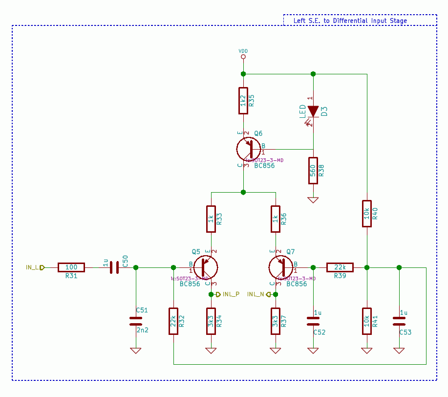
I managed to find some time to try to replicate the EVM's source input. I am having an hard time understanding the input jack schematic, such as the jack's contact and spring seems confusing to me. Anyhow, is this a correct way to implement single ended input?
I have also included a second attachment on what I had for differential input. I am assuming that this would not work at all?
Thanks.
Attachments


Seems fine to me. You might want to have resistors on your (+) inputs from Vmid to further reduce crosstalk and improve immunity to possible EMI susceptibility, like GSM/3G/WiFi. (2k2 were needed here, even the AFE is a bit different)
VMid resistor divider might be more "low-impedance" and get a bit more of capacitance.
(like 1k/1k for the divider and 100uF for Vmid)
While the 5532 is sufficient for the AFE, we had good success with the OPA2134, which is a bit more "immune" to radiation.
Or you leave the opamps out and go the classic BJT way.
Attachments

Thanks again for your expertise Doctormord.
I already ordered the parts but I will get some OPA2134s. I understand that they can be drop in replacements for the NE5532?
Would the differential input circuit in the 2nd attachment work. I want to have diff inputs but am unsure about it due to my ignorance.
I already ordered the parts but I will get some OPA2134s. I understand that they can be drop in replacements for the NE5532?
Would the differential input circuit in the 2nd attachment work. I want to have diff inputs but am unsure about it due to my ignorance.
Yes, they're dropin-replacement but there's nothing wrong to have the resistors on your (+) inputs as well. (if not needed, bridge with zero ohms)
Having more possibilities at initial start makes life easier. dropping them later is easier than fixing a layout by fly-o-wire. 🙂
The diff stage seems fine to me, same as EVM.
Having more possibilities at initial start makes life easier. dropping them later is easier than fixing a layout by fly-o-wire. 🙂
The diff stage seems fine to me, same as EVM.
Last edited:
TPA3251 Dual Application
Hi guys,
I´m working on a 3x BTL configuration using two times the TPA3251.
Now some questions have appeared. Thus I´m very glad to find this thread.
The circuit is to be found here:
View image: tpa3251
1. Since there is no need for a fourth BTL channel, the supply, input and output connections for Channel C & D are left floating. (See 2nd TPA3251 at the bottom) I guess this should be no problem and there will be no fault condition detected. If there is, please correct me.
2. The two oscillators are synchronized, using master and slave mode.
Are they connected correctly? I´m a bit confused of what the data sheet is telling.(polarity etc). Is this synchronisation even necessary?
3. The datasheet suggests a resistor of 3.3 ohms between GVDD_AB/CD and 12V, but it´s placed between VDD and 12V in the evaluation module instead.
Is there a reason?
Thanks in advance 🙂
Regards Fred
From what I recall, when unused channels are present within their class D amplifiers, you should leave the unused channels powered but leave the outputs floating and the inputs AC/cap coupled, to ground. You might want to post on the TI E2E forums about this just to be sure. The engineers over there are usually quick to respond to simple questions like this and are very friendly.
Oscillator synchronisation is provided to make sure that amplifiers are switching at the same time. Even if the oscillators inside each amp are supposed to be switching at say 800kHz they wont be exactly the same. This creates a drift or difference in switching frequency between the two that can easily end up within the audible band. If there is a difference of 1kHz between the two, this can set up a type of 'beating' between the main switching frequency that you can hear and will degrade the audio performance. This is something that you don't want to happen so the option to synchronise the oscillators is provided.
For the best performance TI have provided a differential system for synchronisation (two clock lines in anti-phase). This improves performance by helping to reject any noise/EMI that may contaminate the sensitive and small signal oscillator/clock lines. This is important in a mixed signal application and the differential lines also make the routing of the clock lines on the PCB far less critical than in a single ended application.
As the differential sync lines use two signals this provides the option for two different connections. Either + to + and - to -.... or + to - and - to +. From master to slave. In one case both amplifiers switch on at the same time and switch off at the same time. In the second case as one amplifier switches on, the other switches off etc. Both accomplish the same thing, but the second option could help to provide a more uniform current draw from the supply.
The point of the resistor is to create an R/C network to filter out supply noise from reaching the supply pin it is placed before, or to stop noise from the supplied circuitry from reaching the supply. The chip basically contains two sections of circuitry that require a low voltage supply but for performance issues noise from one cannot bleed into the other.
In the datasheet the raw 12V supply feeds the VDD node with each of the gate drivers being fed from an R/C network.
In the EVM schematic, the raw 12V supply feeds the gate drivers with an RC network being present on the VDD node.
Both will accomplish a similar task of removing what needs to be removed. I can only assume that TI found the EVM solution to be more effective in practise with this device.
This all seems reasonable, thanks for the reply. I will try to get in contact with TI about the floating pins.
- Home
- Amplifiers
- Class D
- TPA3251d2