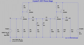
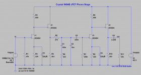
This seems to work out not too bad. Gain is touch and go, but noise and distortion figures are respectable. RIAA accuracy is excellent (+/- 0.2 dB 20-20k with the standard values shown.)
Power supply must be very (very!) low noise. Fortunately the current draw is only 10 mA per channel so it should be do-able. I'll be looking into that in a bit.
Power supply must be very (very!) low noise. Fortunately the current draw is only 10 mA per channel so it should be do-able. I'll be looking into that in a bit.
Attachments
http://www.diyaudio.com/forums/analogue-source/242387-high-octane-phono-preamp.html#post3631742
Got it. Thanks.
I was thinking the voltages were too high to use op amps as the control amplifier, but the schematic shows there are some tricks that can be applied. It worries me a little, though: The voltages are enough to zap the IC if anything goes wrong, even momentarily.
Other options are the Salas shunt, or sourcing a high voltage op amp, or building a control/error amp from discrete transistors
Given the low noise requirements at relatively low frequencies, the usual capacitance multipliers are ruled out - some sort of active (feedback) control will be needed, whether shunt or series.
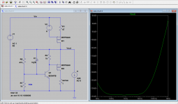
Currently my "object of interest": p-mosfet based shunt regulator, based on the PSU for the Salas phono stage. I simplified it a little replacing the current source FETs with resistors. At 135 dB rejection ratio it's good enough as it is.
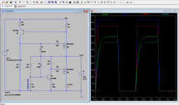
C1 10uF. This gives a turn on time around 1-2 seconds. Turn off is clean with no spikes. The bias V2 will be replaced with a Zener or LED arrangement. Vin 52 Vin is the rectified, filtered DC from 2x18 VAC secondaries connected in series. Telama 60074 for example.
Gate resistors omitted for simulation simplicity. Rsense is just for bookkeeping so I can see how much current is flowing through the shunt arm.
Attachments
Last edited:
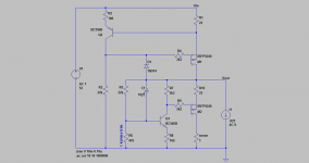
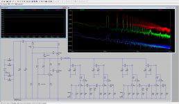
"Crystal M" regulator stage completed as a functioning simulation.
The diode D1 is critical to protect the gate of M1 during shutdown. I also added emitter degeneration R1 R9 ... this degrades the performance but makes the output less critical on the individual device characteristics of Q1 and Q2. Gate resistors R4 and R8 also added for RF stability, though they don't do anything in simulation.
For the bias voltage of the current source MOSFET (M1) I opted to go with transistor-based feedback (Q2/R3) rather than using a Zener or LED to set the bias. I thought this was safer and smarter as it is self-regulating.
The ripple rejection hits -100 dB over the audio bandwidth.
Attachments
One small addition of 22 ohm resistor R10 on the source of M2. This damps out overshoot when the circuit responds to a quickly varying current load. It's very well-behaved now, but unfortunately ripple rejection drops to 72 dB.
Attachments
.. and something of how the regulator would integrate with the filter stages before and after it, with outputs to both stages of each channel.
Attachments
Last edited:
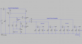
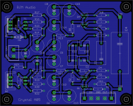
The whole enchilada, as it were.
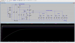
The output power supply ripple is -110 dB at 120 Hz (around -140 dB input referred). Shorting over R10 would reduce that further to below the noise baseline, but I don't think that will be necessary in practice.
The output power supply ripple is -110 dB at 120 Hz (around -140 dB input referred). Shorting over R10 would reduce that further to below the noise baseline, but I don't think that will be necessary in practice.
Attachments
Last edited:
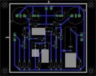
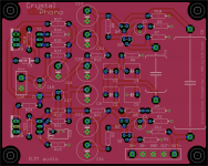
First ideas about the printed circuit board layout. This is what you might call "pre-alpha". Just to get some ideas about how the components might fit together and how much board area things are going to need.
The voltage regulator isn't included yet. I have to decide on whether it will be included or separate, or whether two channels or dual mono.
While clearly the layout could be shrunk considerably from its present state, board area isn't so expensive that it is strictly requires, and larger component spacing makes it easier to build build and modify.
Attachments
The choice of capacitor for the RIAA network (0.1 and 0.033 uF) and interstage coupling (0.1 uF) is very important, both for response accuracy and board space considerations.
I'm very excited about the Vishay MKP1837 metallized polypro film, box type, which are compact, relatively economical, and available in 2.5% and 1% tolerances.
http://www.vishay.com/docs/26017/mkp1837.pdf
With these caps, it should be possible to put a single Crystal channel with the voltage regulator components on a single 8x10 circuit board.
Without them, there is little option but to split the circuit with amplifier and power supply on separate boards.
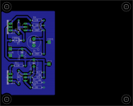
The power supply can be made quite compact. A "pre-alpha" board layout is shown below. The phono stage will cohabit the board in the unused space at right.
I'm very excited about the Vishay MKP1837 metallized polypro film, box type, which are compact, relatively economical, and available in 2.5% and 1% tolerances.
http://www.vishay.com/docs/26017/mkp1837.pdf
With these caps, it should be possible to put a single Crystal channel with the voltage regulator components on a single 8x10 circuit board.
Without them, there is little option but to split the circuit with amplifier and power supply on separate boards.
The power supply can be made quite compact. A "pre-alpha" board layout is shown below. The phono stage will cohabit the board in the unused space at right.
Attachments
Last edited:
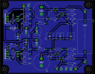
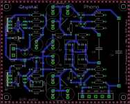
Milestone: Crystal board layout reaches "alpha" revision.
The board is complete and connected, but still far from being ready for fabrication.
One channel, complete with voltage regulation, on one 8x10 cm board. Two boards needed for stereo, plus a power supply (around 40-45 VAC secondaries, rectifier diodes).
Happily there ended up being plenty of room for larger RIAA capacitors, so some flexibility there will be included.
Attachments
With regards for the P-channel MOSFET, pretty much anything should work. TO-220 package is convenient, and low gate charge is preferable. The part should be at least 100 V rated.
Option 1
http://www.irf.com/product-info/datasheets/data/irf9520npbf.pdf
or worst case the big beastie
http://www.irf.com/product-info/datasheets/data/irf5210pbf.pdf
There are a few other parts from IRF in between. They'll all be OK.
IRF9520 is a $1 part at mouser. The only downside is the TO-220 package leaves high voltages exposed on the metal case. TO-247AC case are mostly plastic, but the selection of parts is much more limited.
Hold up. 2N5484 is only rated to Vgs/Vsd 25 V. On power off it would likely fry.
It's vitals are Vgs-off (-0.3 ~ -3) V and Idss (1 ~ 5) mA
Is it time to bite the bullet and go look up some LSK170's?
Obtainable substitutes that I can see are limited to
J202 Vgs-off (-0.8 ~ -4) V and Idss (0.9 ~ 4.5) mA [-40 V breakdown]
J112 Vgs-off (-1 ~ -5) V and Idss (x ~ 5) mA [-35 V breakdown]
whereas the LSK170 is Vgs-off (-0.2 ~ -2) V and Idss ["A"(2.6 ~ 6.5) mA [-40 V breakdown]
Back to the drawing board as they say.
Last edited:
Yes, well, it becomes clear why the 2SK170 is typically used in this circuit.
In terms of voltage gain, the 2SK170 is in a different class than everything else I've looked at. Single stage gains are around 35 dB, where other JFETs struggle to manage over 25 dB.
The problem? Well, for a MM phono stage the ideal total midband gain is 35-40 dB. Which means the single stage gain needs to be 27.5-30 dB. The 2SK170 is too high (just about enough for an MC stage, but...) while everything else is too low.
Once could mix and match the two stages, I suppose. Still, an ideal solution escapes me at present, and that's before thinking about if I can source LSK170s.
Running at lower voltage means 2x12 VAC (24 VAC) to 2x15 VAC (30 VAC) transformer secondaries can be used, which is convenient.
Electrolytic capacitors in the power supply should be rated for 50 VDC, those in the amplifier section at least 35 VDC except for the source bias capacitors which can be 10 VDC.
So little power is dissipated by the mosfets that heatsinking is not required.
Electrolytic capacitors in the power supply should be rated for 50 VDC, those in the amplifier section at least 35 VDC except for the source bias capacitors which can be 10 VDC.
So little power is dissipated by the mosfets that heatsinking is not required.
Attachments
Back to the power supply / voltage regulation for a moment.
Its basic job is to convert the AC line to a clean, low impedance DC power source, but there is lots to discuss behind that one word: "clean" (explaining low impedance will have to wait)
Clean means that the output signal of the audio circuit shows no noise originating from the power supply, because those noise components are lower in magnitude than the noise originating from the audio circuit itself. That's "mission accomplished" for the power supply's primary objective.
Power supply noise can always be reduced, it cannot be removed. It can, however, be buried under broadband noise, where it is hidden from any detection, audible or measurement based.
Phono stages are relatively noisy because they have high gain. "-166 dB" is a good number to remember, it's the broadband baseline noise for 5 nV/sqrtHz. Most competent audio circuits have a input-referred noise value within about 12 dB of that value. Output noise is input * gain, and low frequency gain for a 40 dB MM phono stage is 60 dB. Which means that the output noise floor for a typical phono stage at low frequencies where power supply hum and ripple are most severe is about -106 dB. Any harmonics of at 60 Hz, 120 Hz, 180 Hz, etc. lower than about -100 dB are lost in the general background hiss produced by the amplifier and beyond detection.
That's why for the Crystal amp I've been so fixated in getting the output ripple down below -100 dB on the simulation FFT. This is much harder than for an op amp circuit not because the amplifier noise is less (it's about the same as a NE5534), but because the ripple rejection of the circuit (the fraction by which the power supply noise is reduced by the amplifier circuit itself) is terrible-going-on-pathetic. At low frequencies, the ripple and noise of the voltage supplying the JFET stages must actually exceed -120 dB.
It is important to understand, however, that this is a simple goalpost. Once buried there is no advantage to reduce the noise further. Instead we can look at improving the power supply in other ways, like increasing its output impedance or reducing the amount of filter capacitance.
Last edited:
- Status
- This old topic is closed. If you want to reopen this topic, contact a moderator using the "Report Post" button.
- Home
- Source & Line
- Analogue Source
- RJM Audio Crystal P jfet phono preamplifier | development thread