You are most welcome to do this. Certainly you aren't the first person to think that very rigid construction improves the sound quality.
Meanwhile, I will solder everything neatly to my circuit board.
Thanks for the vote of confidence in the circuit by the way, even though I know the heart of it is borrowed. It's nice to imagine that the troublesome process of matching jfets might actually be good for something tangible.
Meanwhile, I will solder everything neatly to my circuit board.
Thanks for the vote of confidence in the circuit by the way, even though I know the heart of it is borrowed. It's nice to imagine that the troublesome process of matching jfets might actually be good for something tangible.
How to solder - re-solder, new-solder, all equipment, too - a pcb:
Do NOT fill up the hole! Use MINIMAL SOLDER, MINIMAL DIAMETER to connect - better you bend the connections a little bit at the pcb to get fastening or use minimal glue to fix the pieces. Final you have to, you can, you should LOOK THROUGH THE HOLES of the pcb,-!!!
Carrying to extremes: cut the solder-ring (TWO ways) to get ONE way...-)))
Necessary to call "pcb-high-end"-)
After that important public service announcement from cumbb on proper soldering technique, we return to our regularly scheduled broadcast and dive back into jfet suitability.... ")
Vgs0 should be between 1-2 V, and, it became clear later, the beta value (Idss/Vgs0^2) should exceed 0.8 mA/V^2 or there will not be enough gain.
This restriction makes the J113 far more appealing than the other jfets on my list, as the beta tends to be around 6, compared to about 1.5 for the 2N5484 and only 0.5 for the 2N5457 and J202.
The high beta (and reasonably low noise) of the J113 make it a standout part for this circuit.
However, and I'll throw this out as a question: where are the ideal and "still reasonable" operating points for a JFET? It seems the 1/2 Idss (~1/3 Vgs0) is ideal for maximum output swing, but since that isn't such a big concern in this circuit can we move the operating point towards the extremes (to increase circuit gain for example) without penalizing linearity or bias reliability?
Lot's of good information about jfets from Bob Cordell, LSK489appnote.pdf.
Last edited:
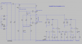
I've gone back and re-jigged the LTSpice circuit to use the J113. The gain is 38 dB with C1,7, about 30 dB without. The phono stage current draw is about 16 mA, while the shunt bleeds 14 mA.
You'll have to copy the J113_RJM model text into your standard.jft library for the simulation to work.
You'll have to copy the J113_RJM model text into your standard.jft library for the simulation to work.
Attachments
Memo to self:
****
For a jfet with I_dss and V_gs0 known, the ideal (1/2 I_dss bias) value of the operating-point-setting source resistor in self-bias circuit is approximately,
R_s = 0.6 V_gs0 / I_dss [or alternatively 0.6 / (beta x V_gs0) ]
The bias resistor value does get smaller when the pinch off voltage increases even for constant beta, but the operating point will usually remain reasonable right to the extremes of the type (2N5484 etc) if the resistor value is calculated off center point values.
****
Generally a given jfet series (2N5484,5,6 or J111,112,113, etc) have fairly constant beta values over the full range. If the value is known approximately, jfets can be quickly sorted by V_gs0 from a single measurement of source voltage, V, obtained with the source resistor R_s as calculated above.
V_gs0 = V + sqrt (V / (R_s x beta))
I_dss can be estimated from V_gs0 and the definition of beta,
I_dss = beta (V_gso)^2
Once binned, matched pairs can be verified using two point measurement or a full curve trace.
****
For a jfet with I_dss and V_gs0 known, the ideal (1/2 I_dss bias) value of the operating-point-setting source resistor in self-bias circuit is approximately,
R_s = 0.6 V_gs0 / I_dss [or alternatively 0.6 / (beta x V_gs0) ]
The bias resistor value does get smaller when the pinch off voltage increases even for constant beta, but the operating point will usually remain reasonable right to the extremes of the type (2N5484 etc) if the resistor value is calculated off center point values.
****
Generally a given jfet series (2N5484,5,6 or J111,112,113, etc) have fairly constant beta values over the full range. If the value is known approximately, jfets can be quickly sorted by V_gs0 from a single measurement of source voltage, V, obtained with the source resistor R_s as calculated above.
V_gs0 = V + sqrt (V / (R_s x beta))
I_dss can be estimated from V_gs0 and the definition of beta,
I_dss = beta (V_gso)^2
Once binned, matched pairs can be verified using two point measurement or a full curve trace.
Latest LTSpice files, and an updated BOM.
I remembered that now I've settled on the J113 the working voltages can be higher since this is a 35 V part.
The circuit can work at 20-25 V when a 2x12 VAC secondary is used. It can work at 25-35 V when a 2x15 VAC secondary is used. The power supply capacitors are rated to 63 V so they don't need to be changed.
According to LTSpice the distortion isn't radically lower, but at higher voltages there is more headroom, and perhaps more important, a wider useable voltage range for the operating voltage. This makes setting the value of the drain resistor a little less critical.
The V+ value is adjusted with the trim pot. As a last resort this can be used to fine tune the jfet drain voltages if they stubbornly end up a bit too low or a bit too high (ideally they should be about 7-9 V). Do not exceed 35 V.
Attachments
A Salas / boozhound with an addition follower after the input stage ?
2SK209 will give you enough voltage headroom and still low noise.
Available from Y to BL grades.
And one can of course parallel matched devices to increase Yfs and reduce noise.
Noise will be the biggest problem.
Patrick
2SK209 will give you enough voltage headroom and still low noise.
Available from Y to BL grades.
And one can of course parallel matched devices to increase Yfs and reduce noise.
Noise will be the biggest problem.
Patrick
Hi Patrick,
Yes, your standard 2-stage passive RIAA but buffering the amplifier stages with followers.
As far as I can tell, the J113 voltage noise of 5 nV/sqrt Hz should put it in the same category as typical audio op amps used in MM phono stages. Not the lowest of low-noise jfets available, but not so high as to be problematic. What am I missing?
My chief concerns are at present, in order of priority,
1. cracking the problem of reliably matching jfets to Rd Rs values with enough room for parameter variance that bins can be used rather than hand-matching resistors to jfets individually. (work in progress)
2. dealing with the circuit's nonexistant PSRR. (largely solved now, by brute force I might add)
3. keeping distortion levels within reasonable limits. (not amazing, but good enough and about as good as the circuit topology allows)
The LTSpice estimate of gate leakage current in the order of 10^-7 A seems reasonable as it is in line with what I have been able to find in published datasheets. I don't have specific info about the J113 however.
Since we aren't building an electrometer here the DC leakage currents don't seem high enough to be troublesome.
re. current sources. Helps the PSRR problem, but makes setting the jfet operating points even more finicky?
Since we aren't building an electrometer here the DC leakage currents don't seem high enough to be troublesome.
re. current sources. Helps the PSRR problem, but makes setting the jfet operating points even more finicky?
I am sure you know how to make a good adjustable current source.
PS
If you change I1 in the Spice file to exactly 3.6mA, Vo1 would be identical to Vo2.
Except that you have (in this simulation at least) infinite PSRR with Vo2.
Patrick
.
PS
If you change I1 in the Spice file to exactly 3.6mA, Vo1 would be identical to Vo2.
Except that you have (in this simulation at least) infinite PSRR with Vo2.
Patrick
.
Attachments
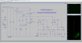
And you can adjust the DC level now at will with the current source.
This is a working full schematics (in Spice).
The only thing missing is a source follower at the output.
Here I would perhaps use a BF862 cascoded by a J111 (also for better PSRR).
I have checked that it has good PSRR as is (by using a 30mV 3kHz sine superimposed on the 36V Vs).
The 6.9V voltage sources are meant to be LM329's and the like.
Distortion at 2V pk-pk is so-so at about -65dB, but that is no surprise.
The nice thing is that it is almost all 2nd harmonics.
Third harmonics and beyond is very low.
Though this is only Spice and not reality.
But I shouldn't disturb your development process any further.......
Cheers,
Patrick
.
Attachments
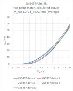
Oh ebay, you bring tears to my eyes!
I've just measured the "Fairchild 2N5457" jfets I ordered from China.
Datasheet: V_gs0 -0.5~-6 V I_dss 1~5 mA
Actual: V_gs0 -4 V I_dss 57 mA
Well, at least the cutoff voltage is in the right ballpark.
I've just measured the "Fairchild 2N5457" jfets I ordered from China.
Datasheet: V_gs0 -0.5~-6 V I_dss 1~5 mA
Actual: V_gs0 -4 V I_dss 57 mA
Well, at least the cutoff voltage is in the right ballpark.
Attachments
Oh ebay, you bring tears to my eyes!
I've just measured the "Fairchild 2N5457" jfets I ordered from China.
Datasheet: V_gs0 -0.5~-6 V I_dss 1~5 mA
Actual: V_gs0 -4 V I_dss 57 mA
Well, at least the cutoff voltage is in the right ballpark.
That one looks more like J112 to me...
- Status
- This old topic is closed. If you want to reopen this topic, contact a moderator using the "Report Post" button.
- Home
- Source & Line
- Analogue Source
- RJM Audio Crystal P jfet phono preamplifier | development thread