Apalon34,
The most interesting thing from without the compensation on so far is that I fat fingered the compliance voltage for the circuit as drawn for the 1541. Running without compensation on it wasn't ~40mV, it was ~400mV of compliance. Ohm made it simple, I messed it up...
Correction - ~40mV was correct. Power supply voltages needed to be bumped to 60 volts to ensure jfets will function...
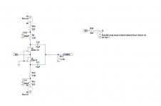
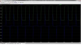
Here is a picture of a "stock" Zen I/V with values figured for a 1541 with no low pass filter. Stimulus is a square wave current of +/-2mA with 200nS rise and fall times. The gates of the jfets are grounded and there is a nice square wave voltage pattern on the input as expected (~40mV or so, see the second picture). I should point out that this rise time represents a 1.75 MHz bandwidth.
I will post the Zin Compensation circuit with and without loop comp in the next reply.
")
Dave
Attachments
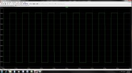
The next picture is of the same circuit with Zin compensation stage added, and with no loop comp capacitor. The gate compensation voltage waveform is on top in the second picture, the input on bottom. The waveforms are offset so that they are easy to see.
As you can see, the input compliance voltage is reduced to <3mV. The spurs on the input are an artifact caused by the phase error I described earlier. They are not ringing, simply a single spike each.
As you can see, the input compliance voltage is reduced to <3mV. The spurs on the input are an artifact caused by the phase error I described earlier. They are not ringing, simply a single spike each.
Attachments
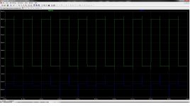
The next two pictures are the circuit with a 1.5nF compensation capacitor added in. This is actually the correct value to match the original Zen I/V roll off at about 20KHz.
As you see in the traces, we have added more phase error into the compensation signal, causing the spikes on the square wave to increase proportionately with the additional phase delay. Still no ringing...
A real circuit will not be nearly so idealized, and likely need some compensation. I look forward to building one soon and am collecting parts for this and a Sabre version as we speak. It will likely be weeks on this end.

Dave
As you see in the traces, we have added more phase error into the compensation signal, causing the spikes on the square wave to increase proportionately with the additional phase delay. Still no ringing...
A real circuit will not be nearly so idealized, and likely need some compensation. I look forward to building one soon and am collecting parts for this and a Sabre version as we speak. It will likely be weeks on this end.
Dave
Attachments
It's alive!
Hi,
Yes, it works! Has been playing for about five minutes now.
I build it in to a philips cd723. Didn't realize this player uses eaij format which gave me some headaches (yes stupid i know) but a converter as posted by member cm solved that. Did give some delay in building though.
A quick scope check suggests that the output isn't that much less then the standard tda1545 used in the player. No weird signals at the output. The unit is still using the badly matched fets. I'll try and solve that next week. voltage at the drain is about 12 volts for the good ones. Input offset below 20 mv. I'll keep track of that but bought some 10r resistors just in case. the coming two weeks will be spent improving the settings.
first impression of the sound? well if it keeps imaging like this, wow!
but now i'm off to celebrate Leiden's relief. Guess i've got a double party...
regards,
Joris
So how does it sound ?
I'm interested by the way you hooked it, if I recall there is some offset at the I out of the converter ... Do you confirm ?
Brds,
nAr
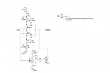
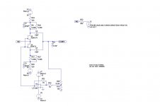
This is a quick & dirty schematics just to show the idea of a cascoded complementary JFET IV.
I hesistated to call it cascoded Zen IV, as it is more of a "Blowtorch IV".
Balanced DAC current is fed to the sources of the input jfets, whose gates are tied to ground.
R2,3,19,21 are bias resistors for the folded cascode MOSFETs (say 200R).
Conversion gain (I to V) is set by R22,24.
One may add additional electrolytic caps to parallel R5,6,16,17.
And R1/18, R4/20 can be replaced by constant current diodes for further improved PSRR.
The rails can now be quick a bit lower than +/-30V.
And the choice is not affected by changes in IV conversion gain and first stage bias.
So one can increase R22,24 (say to 2.4k) and use multiple JFETs in parallel without changing Vsupply.
When using JFETs in parallel, R2,3,19,21 wants to be reduced by N (no.of JFETs in parallel).
No coupling output caps, but consumes quick a bit more current.
Patrick
I think it's a beautiful application of this kind of circuits.Thanks!
If set R2=R3=R19=R21=200 and bias 2SK389/2SJ109 @ 10mA. 2SJ76/2SK216 @ 50ma. With the Rail @ +/-30V,
the 2SJ76/2sk216 gate should be around +/-15V. Then the R5,R6,R17,R16 should be around 6K when we use J508 (2.4mA). We can even use 10K trim
to fine tune the output DV to 1 mV if well match.
Don't know if the quick calculation in my mind is correct?
Also, do you consider to add 2SK246 2SK103 cascoded 2SK389/2sj109?
Thanks,
Search the original blowtorch thread for posts by justcallmedad, and you will find some default values.
I know Borbely uses 2SK246/2SJ103 for cascode, but they just do not have enough Idss to give you sufficient Vds on the K389/J109. For J111/J176, they have anout 35mA Idss, and you can get about 5V vds on the dual fets.
Of course you can use 2SK170/2SJ74 matched pairs instead of 2SK389/2SK109.
The main issue still remains -- input impedance as seen by DAC too high for some DACs, such as PCM1704.
Probably no issue for TDA1543, but then I use passive IV for those......
Patrick
Last edited:
@nar
Hi,
I guess I'd like to consider two kinds of offset here. For clarity i'll try and define them.
The first I'd like to refer to as steady state offset which is there with no signal applied. So far this seems to be determined by the matching off the fet's, drain resistors and psu. This is simple to tweak and i will spend the next couple of weeks trying to get it out. Mr Pass gave the suggestion of using resistors on the gates of the fet's to compensate for bad matching in the article. I'll try.
The second would be the offset generated by signal. The I/V stage has an input imedance so any current fed in to it will result in a voltage. This resulting voltage should not exceed the output voltage compliance as given by the Dac chip manufacturer. This I have not yet measured. The sound so far does not indicate a problem but measurement rules here i think. The output voltage compliance for the tda1541 is 25-30mv i believe so anything below that should be ok. From what i've read so far this is about the voltage to be expected with the tda1541.
Next couple of weeks i'll first try and get the first type as low as i can. After that I'll take a look at the second. I found some 20 hz and 1k&10k sign wave wav files for testing. If anyboody has some square waves or could point me at them, i'll do those to.
Had a couple of hours to listen to the unit this morning and afternoon. It sounds fast, lively and detailed. Compared to what i remember from the 1541+d1 there is a little more emphasis towards the highs. I bit like the difference i heard between the ax and the aleph-j.
However I'm also using a b1 pre in stead of the usual pumpkin and the zen I/V is driven with oversampling whereas the d1 is using nos and 8412 spdif with recloking. Plus i convert eiaj to philips i2s. So a lot of variables to consider. I rigged a coa x cable to use the philips as a transport for the d1 version as well since I only used that on a cd4 or kh7400 before. Did not do that yet.
Regards,
Joris
Question: What is the correct formula to determine the value of the outout filter cap? Right now i used 2n7, guessing that a higher value drain resistor corresponds with a lower value capacitor
Last edited:
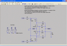
Ltspice file attached.
Cheers,
FFT is giving a -55db 2nd harmonic spike with anything from 2ma-7ma in and 0.5V to 4V out, doesn't seem to jive with the low THD numbers published in the article? What am I missing?
regal,
Try this for the spice directive and see if it gets better... You probably see input voltage offset because the JFET models do not have matched IDS. If someone can fix the models to say 10mA so they appear matched and there is no input offset, it would be appreciated!
.tran 0 10ms 0 10ns
Dave
Try this for the spice directive and see if it gets better... You probably see input voltage offset because the JFET models do not have matched IDS. If someone can fix the models to say 10mA so they appear matched and there is no input offset, it would be appreciated!
.tran 0 10ms 0 10ns
Dave
Last edited:
> Also, do you consider to add 2SK246 2SK103 cascoded 2SK389/2sj109?
BTW in the BT circuit, the folded cascode is already a cascode.
So there is no great advantage to be gained with double cascode, even though it is used at times.
Patrick
Yes. You are right. There really is already a cascode...
For the impedance issue, I am using parallel PCM1704 (2X per channel per phase), it really makes me scratch my head. If roll back to common source in first stage(BT original) , there will be more gain. But it is not common gate and has no benefit from that.
If use common gate, no matter how to cascode it, there is a BIG value output resistor out there...
Add another gain stage and keep output resistor smaller makes it feel redundant.
thinking...
Dual PCM1704 means 1.2k IV resistor at the output, which is not too different from the original BT.
If you are worried about output impedance, then add a source follower (or call it B1 if you must).
For me this is not the real issue. The real issue is still inout impedance too high (15~20R).
Not really ideal for PCM1704.
Patrick
If you are worried about output impedance, then add a source follower (or call it B1 if you must).
For me this is not the real issue. The real issue is still inout impedance too high (15~20R).
Not really ideal for PCM1704.
Patrick
Dual PCM1704 means 1.2k IV resistor at the output, which is not too different from the original BT.
If you are worried about output impedance, then add a source follower (or call it B1 if you must).
For me this is not the real issue. The real issue is still inout impedance too high (15~20R).
Not really ideal for PCM1704.
Patrick
I didn't write it more clearly. My worry is about input impedance too. I think PCM1704 is better connected below 10R. So it doesn't matter how I connect source follower or change from C.G to C.S, it seems doesn't help.Larry
Maybe parallel two 2SK170/2SJ74 (or even four) to lower it?
Then I start worry about the transconductance match (should I)
Larry
I think the best way to deal with th input impedance is to paralell the Jfets. With 36V rails and 500ohm R3&4 it takes the input impedance under 10 ohms. Of course will need a gain stage, but I think it it worth it, 10 ohms is supposed to be the magic number for PCM1704.
One question about the spice model, it seems that for a +-1.2mA DAC the sine i input shoult be set for 1.2mA (Sine 0 1.2ma 1k)? Is that correct?
One question about the spice model, it seems that for a +-1.2mA DAC the sine i input shoult be set for 1.2mA (Sine 0 1.2ma 1k)? Is that correct?
Parallelling JFETs is not always the magic solution. It also creates other problems.
And 500R R3,4 is not going to give you anywhere near enough gain.
IMHO, the whole point of the Zen is simplicity and no active gain stage, as in the D1.
Once you put a gain stage it, you destroy the whole essence of the design.
Might as well stick to the D1.
Patrick
PS Just to illustrate with an example, running a single LU1014 at 180mA with 7R degeneration (for self biasing, i.e. grounded gate) will give you a very linear input impedance below 10R.
Parallelling JFETs is not always the magic solution. It also creates other problems.
And 500R R3,4 is not going to give you anywhere near enough gain.
IMHO, the whole point of the Zen is simplicity and no active gain stage, as in the D1.
Once you put a gain stage it, you destroy the whole essence of the design.
Might as well stick to the D1.
.
But then it is basically a specific PCM63K I/V stage, I don't see any other worthwhile DAC's it would work with as is.
People have been looking for a means to properly integrate a tube into a DAC for about 15 years and I think the Zen I/V with parelelled Jfets and .5Voutput feeding an anode follower fits the bill better than anything I've seen to date.
Parallelling JFETs is not always the magic solution. It also creates other problems.
And 500R R3,4 is not going to give you anywhere near enough gain.
IMHO, the whole point of the Zen is simplicity and no active gain stage, as in the D1.
Once you put a gain stage it, you destroy the whole essence of the design.
Might as well stick to the D1.
Patrick
PS Just to illustrate with an example, running a single LU1014 at 180mA with 7R degeneration (for self biasing, i.e. grounded gate) will give you a very linear input impedance below 10R.
Follow your example, I don't have the LU1014 (Power JFET) datasheet. But I think the high bias current of power JFET will give much higher transconductance. So the input impedance can be lower than 10R.
So if we use MOSFET pair (e.g. IRF610/9610) in the Zen IV or BT circuit. The transconductance could be higher too. So input impedance is lower. I guess it can maintain the simplicity of original beauty.
I really like the simple and elegant style circuit. So please comment.
- Home
- Amplifiers
- Pass Labs
- Zen I/V Converter