Hi all,
i'd like to try an I/V stage with this concept on my AD1865 dac, that actually uses a 200 ohm resistor for I/V conversion, but didn't like the push pull idea (it's difficult for me to find matched 2sk/2sj). Did anyone think that a SE circuit like the one below can work well, even with reduced gain due to the missing negative part of the circuit?
(sorry for the link, didn't got a host that support direct linking)
Picasa Web Album - bonalux.lc8
If there is a chance that it can work i will try it, or any suggestion will be appreciated.
Cheers.
Have a look at this thread. I think it is what you are looking for.
have you compared d1 i/v with zen i/v - winner ?
That is your job.

input impedance is too high and transconductance a bit too low for best current mode output with the sabre.
This is worth a little exploration. As a concept, the R2R ladder
is a linear circuit which should not generate load dependent
distortion. The load resistance does affect the absolute
accuracy of the DAC, but that is not an issue any more
than a slightly lower setting of a volume control.
If a DAC requires a DC output condition, this is easily taken
care of by adjusting the DC potential of the Jfet Gates.
This leaves the character of the Mosfet switches inside the
DAC which drive the R2R ladder. Nominally, saturated Mosfets
are modeled as resistors, but you can figure that they will
not be perfect, and this is where some level of distortion
will creep in. I have not seen any figures as to what the
degradation will be - I suggest that you check it out for
yourselves.
Have a look at this thread. I think it is what you are looking for.
Thank you for the reply, but i don't think it's what i'm, searching for, i guess that the input impedance of that circuit is something in the order of 400 ohm, double of that of my actual circuit. I'm looking for a converter with a very low input impedance (such as the zen, in the order of 15 ohm) to see if the AD1865 is much happier than actually is
but as stated before, don't want the hassle of a push pull topology.For sure i can try it and see what happens, but don't want to fry the AD1865, i don't understand very well the physics of jfet's actually and i'm worried about the negative part of the output current from the dac, if eventually the jfet put out 30 volts the chip is in danger (i think). I need an expert that can confirm there is not the risk to fry a 30 $ chip....
Thank you.
Thank you for the reply, but i don't think it's what i'm, searching for, i guess that the input impedance of that circuit is something in the order of 400 ohm, double of that of my actual circuit. I'm looking for a converter with a very low input impedance (such as the zen, in the order of 15 ohm) to see if the AD1865 is much happier than actually is
For sure i can try it and see what happens, but don't want to fry the AD1865, i don't understand very well the physics of jfet's actually and i'm worried about the negative part of the output current from the dac, if eventually the jfet put out 30 volts the chip is in danger (i think). I need an expert that can confirm there is not the risk to fry a 30 $ chip....
Thank you.
Take a closer look at that thread. It looks like they are achieving input impedance of < 5 ohms with that circuit, with the exact value depending upon selection of FET and bias current. Note that the input impedance of the FET is in parallel with the 400 ohm resistor.
Zen I/V mod to lower input impedance
Hi Nelson,
There is another possible addition to the circuit that might help with some who feel they need the lowest possible input impedance to the I/V.
I believe we can modulate the gates of the jfets with an inverse of the output voltage that represents the voltage modulation caused by the sum of the Iout impedance from the DAC and the Iin impedance seen at the jfets. We have, at least in appearance, reduced the input impedance by well better than an order of magnitude, perhaps more depending on device matching and tracking throughout the circuit. overall performance of the I/V stage itself appears unaffected.
I will add an example in a second post. I look forward to any feedback.
Dave
Last edited:
Circuit examples and details - I used an inverted, divided and buffered version of the output waveform (shown in this proof of concept example as a balanced Zen I/V with a follower for the feedback buffer, can be done with an inverting opamp as well for single ended I/V). This is feeding the gates to the jfets and should be low impedance and as noise free as possible with bandwidth comparable to a the IV stage.
The output 4.7nF cap presents a significant phase error for this feedback, so it is removed. Low pass filtering should be done down stream as shown. Without the 4.7nf cap, the small remaining phase error in the feedback still imposes some impedance nonlinearity, but because we are talking a total apparent impedance at the I/V of around ~0.2ohm or less, it appears to have very little or no effect on the output.
I know the additions could be considered as a departure from the Zen tradition... The original D1 had a follower included so the addition of one for the filter and one for the feedback here isn't too far of a stretch.
Still need to build one. I will probably add it to the "Group Zen" I/V stage in the other post and start from there.
Please let me know if anyone sees any major issues!
Dave
Attachments
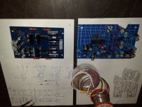
build report, getting there
Hi all,
The past couple of weeks i've been busy building. I'd like to make a disclaimer here in stating that funds are low and I need to do as much as i can do with what i have at hand. Thus i am limited to using the tda1541 I have, appropriate or not. Therefore i went straight to 2k resistors in the loads and a +/- 40 V supply. to be sure i also included the buffer as proposed by Juma but using sk170's instead. I kept with the original output caps to be able to compare (two points for taking the output signal).
I've got the circuit up and running and here are my first observations:
-keep the supply voltages well regulated and equal between plus and minus. any difference seems to result in offsett in voltage and current, thus relating in to offset in input voltage etc.
-those fets do need to be well matched. I thought i matched nicely but apparantly did not. (if someone has a nice matched quad i'm game...)
-give the circuit time to heat up. the offset goes down. (I've got 2 and 6 mv at the input. fet's are V-grade though and voltage at the drain is a bit low).
Anyway, im about ready to give it some signal and listen to it. this i will do the coming two weeks. Does anybody have some hints what to look for and what to measure? I've got an old analog (tube) scope and a simple function generator at hand. Files for burning to cd and testing would be welcome.
Anyway, as soon as i get some sound out of it i'll report. Got a D1 to compare with using a 1541 as well.
regards
Joris
Attachments
I think you deserve a prize for the first person to build it.
I look forward to hearing your impressions.
I know nothing about DAC's, but I wonder if you paralleled 4 x tda1541's together, whether the input impedance of the I/V converter would be less of an issue.
i think if you parallelled the outputs of the DAC's the impedance issue would get worse.
need more I/V fets in parallel to reduce the impedance.
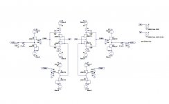
Zen I/V for the 1541
Hello all,
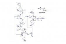
Several people showed an interest in using the Zen I/V with a 1541 and that the datasheet states to keep the voltage compliance for the current out at 25mV P-P or less. I have an interest to try one of these so I thought I would share a circuit that is optimized for this chip and addresses this datasheet requirement.
This is just like the circuit described in post 170 of this thread. It uses the output of the I/V converter to modulate the gates of the jfets, causing the impedance of the converter to drop significantly without any significant changes to the output.
I modeled the source impedance of the 1541 as 800 ohms. I do not know what this actual output impedance is from the chip but the component values as-is will probably be pretty close. If someone has this specification, let me know and I will update it.
As depicted, the voltage compliance into the input went from about 40mV P-P with no compensation, to about 4mV P-P. Use 1/2W resistors everywhere to make it simple. You might also want to use four 13K 1/2 W resistors in parallel in place of the R1/R10 and R2/R11 pairs to add extra power dissipation headroom.
I hope someone will check the work here and let me know if there is anything amiss. I can't wait to try it out see what it sounds like with this combination of DAC chip.
Dave
Hello all,
Several people showed an interest in using the Zen I/V with a 1541 and that the datasheet states to keep the voltage compliance for the current out at 25mV P-P or less. I have an interest to try one of these so I thought I would share a circuit that is optimized for this chip and addresses this datasheet requirement.
This is just like the circuit described in post 170 of this thread. It uses the output of the I/V converter to modulate the gates of the jfets, causing the impedance of the converter to drop significantly without any significant changes to the output.
I modeled the source impedance of the 1541 as 800 ohms. I do not know what this actual output impedance is from the chip but the component values as-is will probably be pretty close. If someone has this specification, let me know and I will update it.
As depicted, the voltage compliance into the input went from about 40mV P-P with no compensation, to about 4mV P-P. Use 1/2W resistors everywhere to make it simple. You might also want to use four 13K 1/2 W resistors in parallel in place of the R1/R10 and R2/R11 pairs to add extra power dissipation headroom.
I hope someone will check the work here and let me know if there is anything amiss. I can't wait to try it out see what it sounds like with this combination of DAC chip.
Dave
Attachments
Last edited:
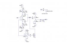
I realized that the low pass filter on the output was missing something...
R15 has been added in the picture to allow the 4.7nF cap to do the job it was intended for! Since it has been moved past the follower to reduce the phase error for the compensation circuit, we can no longer rely on the output impedance from the I/V converter (500 ohms as drawn in Nelson's article) for the "R" in our RC filter.
This is also true in the balanced version I posted here. Add the resistor if you want an LPF at the output, otherwise remove the cap.
Dave
Attachments
Thank you both for the feedback. I appreciate other eyes on the idea and want to make sure it is sound. It also gives us more opportunity to discuss the circuit!
The values in the resistor divider are chosen to inversely modulate the input voltage offset to level just below the point of adding any feedback (i.e. the inverse voltage offset added by the compensation is just slightly below the input compliance voltage modulation created by the input current * input impedance of the jfets).
Once you cross that threshold, the input impedance does go negative and act a little wonky, but output effects in the I/V are still below the noise in the simulation. There appear to be no single frequency effects created. I cannot attest to multi-tone or intermodulation effects which is why I first thought to keep the phase error in the feedback circuit to a minimum. Probably not necessarry, after all, we are talking milidegrees...
If the goal is to cancel the impedance induced voltage compliance changes at the input to the circuit, any induced effects from the compensation should be far smaller than actual or perceived degradation in DAC performance driving into a less than ideal I/V input. Here is the question I would like to answer - Can we hear the difference?
Having this HF compensation cap in place would eliminate the need for the RC after the follower for low pass filtering, and likely improve the performance of the output follower a bit.
I still need to build one of these to see how much HF compensation the real circuit will need.
We need it to work throughout the audio frequency range as the impedance compensation is input frequency dependent. Adding a pole to roll off at 1Hz defeats the purpose of the added circuitry.
Thank you both again for the input. I look forward to more conversations about it.
Dave
I did give quite a bit of thought to how input feedback effects in the voltage domain might effect the current domain performance.Be careful with the circuit driving the gates of the jfets, because it is a form of positive feedback.
The values in the resistor divider are chosen to inversely modulate the input voltage offset to level just below the point of adding any feedback (i.e. the inverse voltage offset added by the compensation is just slightly below the input compliance voltage modulation created by the input current * input impedance of the jfets).
Once you cross that threshold, the input impedance does go negative and act a little wonky, but output effects in the I/V are still below the noise in the simulation. There appear to be no single frequency effects created. I cannot attest to multi-tone or intermodulation effects which is why I first thought to keep the phase error in the feedback circuit to a minimum. Probably not necessarry, after all, we are talking milidegrees...
If the goal is to cancel the impedance induced voltage compliance changes at the input to the circuit, any induced effects from the compensation should be far smaller than actual or perceived degradation in DAC performance driving into a less than ideal I/V input. Here is the question I would like to answer - Can we hear the difference?
With no compensation cap on the COMP+ node, it falls off very gradually above 100KHz. I tested with values from 47pF up to 470pF in this location. At 470pF, we are back to a very similar roll off to the original circuit on the high end, around 20KHz. With this 470pF cap in place, the input voltage compliance went from ~2mV at 1KHz to about 3mV at 20KHz. Still very good considering the circuit without compensation was ~40mV or so...It will probably need some frequency compensation to be stable and as such, it's influence will diminish with the frequency, raising the input impedance.
Having this HF compensation cap in place would eliminate the need for the RC after the follower for low pass filtering, and likely improve the performance of the output follower a bit.
I still need to build one of these to see how much HF compensation the real circuit will need.
Regal,Yea, I think you want that servo to work only below 1hz, you need a cap on it ?
We need it to work throughout the audio frequency range as the impedance compensation is input frequency dependent. Adding a pole to roll off at 1Hz defeats the purpose of the added circuitry.
Thank you both again for the input. I look forward to more conversations about it.
Dave
Did you look at the behavior with fast rising signals, like the 200ns from the pcm1704 ?
of course this is a worse case, but the usual problem invoked with the op-amp way to do is that it can't handle fast rising signals correctly.
Apalon34,
No, not yet. That's a good point. I will
I will also include an example of what the circuit does without the impedance compensation control as well.
The most interesting thing from without the compensation on so far is that I fat fingered the compliance voltage for the circuit as drawn for the 1541. Running without compensation on it wasn't ~40mV, it was ~400mV of compliance. Ohm made it simple, I messed it up...
If anyone knows what the output impedance for the 1541 is, let me know and we can make the model more accurate.
I will finish up and post some results later to look at.
Dave
- Home
- Amplifiers
- Pass Labs
- Zen I/V Converter