> continue at this rate and i'll have to rename it to EUVL DAC
a) It is an IV and not DAC.
b) It comes from Mr Curl and not me.
c) I am already into version 4 of this, and the one published is version 0.
And no, I do not publish work in progress. Sorry guys.
But Version 0 sounds real nice. Just too much current.
Patrick
PS I do not use sigma delta DACs, but Sabre is one, though you need to have high bandwidth IV to match.
Thanks..
a) b) c)
a) the DAC3 has already been modified to discrete DIP8 Class A opamps, with BT style I/V's added there's just the DAC part left to alteration.
b) using the line stage of the BT as an I/V wasn't JC's, was it ?
c) the thought counts, not the version.
Hi,
Thank you mr Pass!
I'm up to matching Fet 60 and the j74 batch is promising. PSU is about ready but will be lower (only got a 2x22v trannie and don't want to use a voltage doubler yet). If only i could find my tda1541's...
Thank you Tea bag as well for first mentioning this idea!
regards,
Joris
frantically searching for his 1541's and wondering which cdp to use for a platform...
....searching for his 1541's ...
Zen I/V might not not be ideal I/V stage for TDA1541. That DAC chip prefers lower Zin of the I/V stage. 15 ohms at Zen I/V input creates 30mv at TDA1541's output which is too much and degrades the chip's performance.
Also, with 1k in drains of Zen I/V you'll get just 1Vpeak (TDA1541 outputs +/-2mA), so you'd have to adjust gain/PS voltage...
Zen I/V might not not be ideal I/V stage for TDA1541........
also fact that TDA1541 is sinking 2mA ..... so few more bits & pieces
certainly solution for 1541 needs some cascoding , buffer too ..... but that is already covered in these two treads
No, that's not what I was talking about. There are more DAC technologies available than just ∑∆ and R2R. I am talking about a parallel DAC without resistors, which uses scaled transistor sizes to handle binary-weighted conversion. I guess you could call it an I2I instead of R2R. Since each bit is being used to switch a large chunk of fixed current, the chip actually works better with the two complementary (balanced) outputs, because that way the current is never shunted - each bit of current always goes to one output or the other. The particular chips I have worked with have variable total current, from 2 mA up to 20 mA, so the I/V follower must be specifically designed to match.You are talking about Sigma-Delta technology, surely one would build this new I/V with a proper R2R chip.
But you didn't answer my question. Why would you need 3 DAC chips? (2 extra) - there are certainly balanced output DACs that are not ∑∆.
Hi Guys,
If anybody is going to design a PCB for this, please consider making it differential. Too many good DACs have differential outputs. Schematic for a differential IV has been posted earlier in this thread.
Secondly, consider including a balanced/differential to single ended converter. This way this board can serve as the entire ouput stage for a DAC with no opamps in it.
Dear Papa,
Thank you very much for this wonderful gift. Despite your generosity, our greed does not end. Can you please consider giving us a blessed balanced to single end convertor?
Thanks in advance,
Dinesh

Thanks Nelson
I was turned off from that idea because of the requirement for having to use bigger voltages because of the extra current draw and therefore higher voltage drop.
Then my brain turned on just then. I can parallel parts with Idss of 3mA to 4mA instead of 10mA.
So no need to increase voltages.
Thanks Nelson for making me look at this option again.
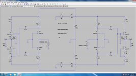
Zen design I/V
In the design given, I never like to see a chip driving external devices with voltages that may drive current back into the chip until the power becomes stable. I would expect to see parallel diode limiter to ground at the input. Reliability requirements trump minimum parts count and cost in well designed equipment.
In the design given, I never like to see a chip driving external devices with voltages that may drive current back into the chip until the power becomes stable. I would expect to see parallel diode limiter to ground at the input. Reliability requirements trump minimum parts count and cost in well designed equipment.
2SK170/2SJ74GRs are a bit difficult to find, but going to 3mA Idss is the correct move if you do not want to cascode. Also Yfs is (quite a bit) lower at 3mA than at 10mA, so it is not a 1:1 gain by paralleling. And your capacitances go up 1:1. So perhaps higher voltage is still the easier solution.
For your simulated circuit, you should consider changing :
1) C1,2,5,6 to 10uF minimum
2) R8,16 to 10k (using 500ohm to drive a 1k load is a bad idea)
3) add caps (100uF) to gnd after R9,10,17,18
I would use a complimentary follower with a single pair of 2SK170/2SJ74 and no source degeneration. Hardly any distortion with 10k load.
Patrick
You are right patrick but there is a reasonable benefit in going for lower idss devices.
If you look at the data sheet a device with Idss of 10mA has a transconductance of 40mS, but a device with Idss of 3mA has transconductance of about 22mS if I parrallel 4 I get transconductance of 88 with a current draw of 12mA.
So I get more than double the transconductance (ie less than 1/2 the input impedance) with only 20% more current draw.
I will have a look at switching devices. I didn't know there were complimentary devices available or are you suggesting I build a D1 type circuit with these jfets.
- Home
- Amplifiers
- Pass Labs
- Zen I/V Converter