Well, yes and no. Nobody in his/her sane mind argues with Kirchoff's Law.
However, we live in EMI jungle. The floating power supply is an RF antenna, and through parasitic capacitances the RF it receives gets fed into the circuit.
You probably know better than I that an ungrounded shield is practically always worse than no shield at all. Your floating power supply is like an ungrounded shield.
Maybe in the final overall shielded I -> V converter it is not a real issue. But one should not blindly adopt floating supplies - everything has its price.
...
If one looks at/into isolated power converters dataheets, he/she can see (e.g. VB-053R3S2 datasheet, Pinout ,application circuits Power Modules DC-DC Converters 2W 2:1 Regulated Single & Dual Output ) : "I/O Isolation Capacitance 60 pF".
Its one of the reasons I'm planning battery power with no charging circuit (i.e. pull the batteries and use a proper charger) that way you don't have a bigger antennae. I definately recommend grounding the jfet heatsink, the battery cases and the cap cases (scratch a pair spot and solder a wire to true ground). Also with the power for the DAC; the torroids and rectifiers will be in a separate chassis. Mian source of RFI would be the digital side of the DAC and that is generally going to end up in any I/V stage no matter what, iow's dealt with the post i/v filter. Any other tips to deal with this?
I'm planning on a bessel after the Sen then a DCB1, surprised this hasn't been brought up, especially with some of the high speed DAC chips folks are working with.
RM idea sniff test
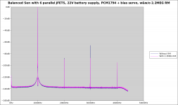
I gave this a go on a breadboarded Sen. It seems to work. This is the first Sen I've made which I think would hit -90dB THD+N.
The effect of RM is more significant at higher frequency so I've attached a comparison of the 10kHz spectrum before and after the RM mod.
I listened to it briefly and it seems to be OK.
RM1, as shown, looks like a fix for the gate capacitance issue and would allow you to parallel up more JFETs.
Simulation shows significantly reduced 3rd harmonic distortion.
I'll try it out shortly.
I gave this a go on a breadboarded Sen. It seems to work. This is the first Sen I've made which I think would hit -90dB THD+N.
The effect of RM is more significant at higher frequency so I've attached a comparison of the 10kHz spectrum before and after the RM mod.
I listened to it briefly and it seems to be OK.
Attachments
Its one of the reasons I'm planning battery power with no charging circuit (i.e. pull the batteries and use a proper charger) that way you don't have a bigger antennae. I definately recommend grounding the jfet heatsink, the battery cases and the cap cases (scratch a pair spot and solder a wire to true ground). Also with the power for the DAC; the torroids and rectifiers will be in a separate chassis. Mian source of RFI would be the digital side of the DAC and that is generally going to end up in any I/V stage no matter what, iow's dealt with the post i/v filter. Any other tips to deal with this?
I'm planning on a bessel after the Sen then a DCB1, surprised this hasn't been brought up, especially with some of the high speed DAC chips folks are working with.
I think that in another thread i have already suggested charging circuit which connects through relay to the accumulator to be charged. Relay contacts can have very low capacitance, so extra EMI from antenna represented by the charging circuit will be very small.
L = 10mH Fastron 77A series
DCR = 12R
dV ~ 0.5V @ 45mA
C = 10000uF 16V Vishay BC 056 Series
f_RC = 1.3Hz (1st order)
f_LC = 16 Hz (2nd order)
Patrick
To reduce any high frequency noise that might remain.
In any case no harm.
Patrick
What is parasitic capacitance of "L = 10mH Fastron 77A series" ? I.e. can one be sure truly HF noise is going to be blocked ?
What is serial resistance of "C = 10000uF 16V Vishay BC 056 Series" ? I.e. can one be sure truly HF noise is going to be blocked ?
And what are antenna capabilities of apparently not small in physical dimensions "C = 10000uF 16V Vishay BC 056 Series" ? I.e. can one be sure that the thing won't suck in more HF noise ?
I believe, meaning that rechargeables are more eco-friendly than primary batteries.
The "battery" word does not automatically imply "rechargeable"; there was no "rechargeable" word in the post I quoted.
What is parasitic capacitance of "L = 10mH Fastron 77A series" ? I.e. can one be sure truly HF noise is going to be blocked ?
What is serial resistance of "C = 10000uF 16V Vishay BC 056 Series" ? I.e. can one be sure truly HF noise is going to be blocked ?
And what are antenna capabilities of apparently not small in physical dimensions "C = 10000uF 16V Vishay BC 056 Series" ? I.e. can one be sure that the thing won't suck in more HF noise ?
Most of the earlier results I posted had a small ground loop going through the servo.
For reference, having fixed that, I now have a balanced Sen implemented on a breadboard with no shielding and I get:
THD+N: 0.0063% or -84.0 dB
as calculated by the script here: https://gist.github.com/246092/dd9f7ffcaee42d1e1733e1280d3c77439fae951c
If I modify the script to exclude more of the skirts (from clock jitter?) I get -86.8 dB.
I really don't think you need to worry so much about noise. Just make sure there are no ground loops and put it in a box.
Attachments
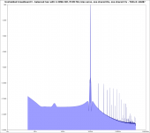
-90dB THD+N
I modified the script to have a notch filter from 0.725 f0 to 1.38 f0 which according to some comments in the script is more like an AP1.
This gets rid of a lot more of the skirt of the fundamental.
With the new script and a new measurement taken later at night with a bit less mains hum I now get:
Analyzing "1k5-4.flac"...
Frequency: 999.902450 Hz
THD+N: 0.0021% or -93.5 dB
So there's your -90dB and it's still on breadboard outside the box.
If I modify the script to exclude more of the skirts (from clock jitter?) I get -86.8 dB.
I modified the script to have a notch filter from 0.725 f0 to 1.38 f0 which according to some comments in the script is more like an AP1.
This gets rid of a lot more of the skirt of the fundamental.
With the new script and a new measurement taken later at night with a bit less mains hum I now get:
Analyzing "1k5-4.flac"...
Frequency: 999.902450 Hz
THD+N: 0.0021% or -93.5 dB
So there's your -90dB and it's still on breadboard outside the box.
Gibbs phenomenon is about a different thing actually.
It like this. If you take classic (not DFT, but based on integral) Fourier transform, it uses (as well as DFT) the concept of so called orthogonal functions. I.e. input signal is mapped into superposition of the orthogonal functions.
When this is done, a so called norm is used to estimate the mapping quality.
Th norm is:
integral_from_minus_infinity_to_plus_infinity((Fin(t) - Fout(t)) ^ 2)
.
Or, in simple English, is the area of the difference curve. Now, pay attention to the word area.
When a rectangular function is approximated with infinite number of harmonics as it should be, the spikes are about 9% (IIRC) high, but with zero width.
Since the width is zero, the spikes area (which is the deviation from what input function as we, humans, see it) is, of course 9% * 0 == 0. Zero.
So, in terms of the adopted norm (see above) the approximation is perfect - despite the spikes. I know this sounds odd, but for Fourier transform it's the definition of norm - area and not absolute deviation at any given point.
Hi Patrick
I've installed and assessed my new Jensen tranformer-based balanced input in my preamp, so I'm close to giving SEN a go with my Buffalo DAC.
One thing is confusing me. You suggested using some Fastron chokes and 10000 u/16 V caps to filter the battery supplies (I've bought some of the chokes, and have some Panasonic FC 8200 u/16 V caps). But how to best arrange the LC filters? Did you mean- for each individal 18 V supply-
one series choke (in the + or - ve line) and a parallel cap after the choke between the + and -? (Probably not, as cap V rating exceeded)
two series chokes (in the + and - ve line) and a parallel cap after the chokes between the + and -? (Probably not as cap V rating exceeded/marginal, and series V drop > 0.5 V you mentioned)
or did you mean the a LC filter to ground? (?!). One per supply, or two?
Thanks
Paul N
BTW thanks for the simulations you did. I've learnt a lot from them")
I've installed and assessed my new Jensen tranformer-based balanced input in my preamp, so I'm close to giving SEN a go with my Buffalo DAC.
One thing is confusing me. You suggested using some Fastron chokes and 10000 u/16 V caps to filter the battery supplies (I've bought some of the chokes, and have some Panasonic FC 8200 u/16 V caps). But how to best arrange the LC filters? Did you mean- for each individal 18 V supply-
one series choke (in the + or - ve line) and a parallel cap after the choke between the + and -? (Probably not, as cap V rating exceeded)
two series chokes (in the + and - ve line) and a parallel cap after the chokes between the + and -? (Probably not as cap V rating exceeded/marginal, and series V drop > 0.5 V you mentioned)
or did you mean the a LC filter to ground? (?!). One per supply, or two?
Thanks
Paul N
BTW thanks for the simulations you did. I've learnt a lot from them
Battery+ is connected to Inductor connection 1.
Inductor connection 2 to Cap+.
Cap- to battery-.
The SEN circuit is then supplied by taking V+ from Cap+, and V- from Cap-.
My mistake about the voltage, terribly sorry for that.
Should have been 25V. I was thinking about my ES9022 which uses 9V supplies.
If you have already bought 16V Caps, you may use 2 of them in series to give you 32V.
Alternatively reduce the battery voltage to 15~16V.
(e.g. by dropping the voltage with 3 diodes like 1N4002 or a single 1W 47R resistor in series before the L+).
The circuit still works just fine with 16V.
Patrick
Last edited:
Hi Patrick
That's what I thought you meant- no other interpretation entered my head- until I noticed the cap's V rating. No worries. I had the FC's left over from another project. It also means I have the correct number of chokes!
I'm going to use a 16 x AAA NiMH per supply. So the average voltage will be (16 x 1.3) - 0.5 = 20.3 V. I'll adjust R1 to 655k to suit
My only concern is dc on the output. Ideally, I need to keep the differential dc to within +/- 50 mV. With my intended arrangement, the dc to ground on each outout will vary by +/- 175 mV as the batteries discharge. But hopefully, if I charge all the batteries fully to start with, their discharge rates will match closely enough to keep the differential dc within acceptable limits
Nic- it will take a little time yet! Patience....
Some might be interested in my findings here-
pink fish media - View Single Post - Buffalo II - Assembly for the Electronically Bewildered.
Although they concern input transformers fed from Legato, they may be relevant to SEN used in this way
Paul
Battery+ is connected to Inductor connection 1.
Inductor connection 2 to Cap+.
Cap- to battery-.
That's what I thought you meant- no other interpretation entered my head- until I noticed the cap's V rating.
No worries. I had the FC's left over from another project. It also means I have the correct number of chokes!I'm going to use a 16 x AAA NiMH per supply. So the average voltage will be (16 x 1.3) - 0.5 = 20.3 V. I'll adjust R1 to 655k to suit
My only concern is dc on the output. Ideally, I need to keep the differential dc to within +/- 50 mV. With my intended arrangement, the dc to ground on each outout will vary by +/- 175 mV as the batteries discharge. But hopefully, if I charge all the batteries fully to start with, their discharge rates will match closely enough to keep the differential dc within acceptable limits
Nic- it will take a little time yet! Patience....
Some might be interested in my findings here-
pink fish media - View Single Post - Buffalo II - Assembly for the Electronically Bewildered.
Although they concern input transformers fed from Legato, they may be relevant to SEN used in this way
Paul
The output DC has nothing to do with the bias, or current supplied by the battery, or the voltage of the battery itself.
They are in a separate current loop.
The output only sees current looping from the DAC I_out back to the DAC Gnd.
And the battery is not connected in ANY way to this loop.
Your output DC therefore depends on the Vref stability and any internal drift of the DAC.
I am assuming you intend to use ES9018.
Don't take my word, ask Nic. He has first hand experience.
Patrick
Hi Patrick
I'm sorry, this is a case of me being (selectively) thick. I wasn't being deliberatively contentious, I was just being incorrect! I mistakenly thought the ratio of R1 to R2 affected the dc output voltage. But you say, how could they?
Perhaps you could re-explain the role of R1 and R2? In your original article, I think you mentioned they were concerned with switch on behaviour. In the circuit adapted for ESS9018, I can see that their ratio is such that, were the 18V supply referenced symetrically about the input reference, 1/2 VACC, they would serve to keep the output voltage at ground. Why? (The exact ratio required to do this varies with input reference voltage, and supply voltage, and it was this that led to my erroneous comments in my last post)
I'm missing something and it's driving me mad
Thanks
Paul
Paul,
I was just trying to explain to you.
If I somehow gave you the impression that I was impatient, I apologise.
As you quite rightly notice, a DC offset at the output is only possible if a current can pass through the R_iv and return to the DAC Gnd.
So this current can only come from the DAC i_out.
That is the output side.
The problem is that we also want the input side to be either 0V, or at a specific value, say Vref.
And this is only the case when the current through the top FET is at Idss, such that Vgs = 0.
In case of (Idss) matched FETs for top and bottom, the condition requires that Vds for both FETs are largely equal.
Idss is much less sensitive to Vds than Vgs, but it still is.
So in order to make sure that you don't get a significant DC offset at the input side, you need to make sure they have about the same Vds.
This is the role of R1 & R2.
So suppose we design R1 & R2 at 1.3V, but the battery is at 1.4V at the start and 1.2V at the end.
How much input offset do we get ?
I changed the supply voltage from my model from 18V to 20V, and then also to 16V.
This is a even higher % voltage change than a NiMH battery will experience.
At least according to Spice, when you use matched quads of 2SK369V, the offset at the input is +/- 0.000025V.
Or a total of 50µV when Vs changes from 16V to 20V, using the same R1 / R2 values as in 18V case.
For the case of the ES9018, things gets a bit complicated, because the output current is affected by the input offset to an extent.
Using the equivalent circuit, this DAC output current offset is equal to [input voltage offset / 781.25R].
And since we use a 680R R_iv, the voltage offset induced at the output is therefore 22µV.
Quite some difference from the 175mV you were worrying about.
And even if Spice is wrong by a factor of 100, I think you still should not loose any sleep.
Patrick
Last edited:
In practice, with ES9018 and the SEN, I went from 2x 9V NiMH batteries (18V nominal) to 3x 9V NiMH batteries (27V nominal) without bothering to change R1/R2 (chosen for 16V) and the change in DC offset on the output was <5 mA (as far as I recall).
I am now running at 22.5V (regulated) and the output DC offset is stable, below 1 mV, and I still did not change R1/R2. It may be as much as 6-7 mV at cold start, but it settles in a couple of minutes (I guess when the FETs reach equilibrium temp).
I will eventually change R1/R2 to their correct values, but for the moment I'm just enjoying the music
Cheers,
Nic
- Home
- Source & Line
- Digital Line Level
- Zen -> Cen -> Sen, evolution of a minimalistic IV Converter