My suggestion for this was to adjust the bias on the LTP so as to move the collector of the LTP output up or down slightly.
From what I can tell, the 545 basically uses the output DC bias of each previous stage to set the bias of each subsequent stage (together with other components.)
The single ended signal finally gets split through an inverting unity gain stage and applied to the output stages. If the DC level of the two signals feeding each side of the Class B output stages is off, then the outputs will reflect that with a DC offset. I think the VR602 POT in the circuit is supposed to control that.
Prof: have you tried adjusting that pot?
VR602 sets the quiescent bias for the output devices.
I shall try trimming the LTP tail resistor as you had suggested earlier ...
... I could do with a bit of "hand-holding" from the "circuit surgeons" there... my LTP devices match is not close...all I wish to do is to tweak that manually and leave it there...
OK. Pay close attention. The DC offset in the 545 arises because the input DC levels at Q619 and Q621 are incorrect. If one is higher than the other you will get crossover distortion AND a DC offset. If they are both too low, too will get crossover distortion, but no offset, and if both are too high, then you will have some Class AB operation (not a bad thing), but too much that and the amp will just be dissipating power as heat and cooking the output stage, since both the positive and negative sections will conduct at the same time.
The match of the input transistors (the LTP) is irrelevant to the offset in the 545. it is critical to the small signal performance of the amp, but it is not apparent that it can cause DC offset. So, if your concern is offset, then forget about the LTP. (but once the amp is working, don't forget to match them, or it may sound like crap).
It appears that Q605 and Q 615 are current sources, stabilized by diodes D105 and D107.
After the circuit involving Q617 (ending at R647 and R 649), the circuit is entirely complimentary (symmetrical for positive and negative sides), so any imbalance between them must be introduced at the point where the single ended signal splits to drive the complimentary output stages.
That split occurs at the collector of Q613. One branch goes to Q619, and the other goes to Q617 (I do not yet understand why Q617 is an emitter follower, since we need some sort of phase inversion at this stage to drive the negative side). I suppose if the input signal swings full positive and then full negative, one side will just go to zero while the other turns on, but man, that's a crappy approach...destined for crossover distortion...
Anyway, it really looks like the trim pot VR601 is there to adjust the bias between the two output sides.
Have you tried adjusting that? Do you know if it is actually working?
If the pot is shot, then you will maybe get some negative cycle swing, but it will be distorted. If Q617 is shot, then you may get some leakage signal through the pot and R643 to drive Q621, but again it will not be the same level as the positive cycle.
Try measuring the voltages at the input side of Q619 and Q621. They should be near zero, and if there is any voltage they should be the same and opposite polarity.
It is important to note that up to the output collector of Q613, there is only one signal path, so there're is no opportunity for any imbalance there. Once that signal path splits, them difference can arise that will result in DC offsets.
Here is the relevant section of the circuit:

Last edited:
Hi cogeniac,
There didn't seem to be any interest at the time. You did a good job and those that wanted one seemed to be serviced by you just fine.
At this point, I am perfectly fine if you offered your board to them. The design I gave to everyone here, but I think it would be a great service for everyone if the store did offer it. You worked at this as well, and that board is your design. So if they offered you anything to use it, I am totally cool with that. I would simply like to see it easily available to members and maybe some good service techs might pick one up. It would allow them to do better work.
-Chris
If I made it available, I would not expect any return. Earning a few bucks a month would just be an accounting headache. I'd rather folks on the forum had the tool. What's the process for offering it?
@ Cogeniac:
Much gratitude from my side for your time and effort...
I shall study that and act accordingly.
Yes, the Vbe transistor is good and the bias pot is working correctly- I could set the quiescent current as per recommendation.
The issue basically is once the servo is active, the amp is stable more or less, but swings to a high offset in a random fashion. Once the DC servo is taken out for test purposes, immediately the offset swing appears, though to a lesser level.
(I don't have a variac, but I use a multi-watt/multi-bulb/switch combo for protection. I am also thinking of a speaker protection relay circuit, under the circumstances.)
Prof:
That description helps. So the issue is not that you can't adjust the bias, the issue is that the bias changes randomly, so the servo is often working, and sometimes cant control it.
It is not worth trying to get the servo to do more. It was never intended for that and as Anatech notes, it should not really even be necessary. You need to find the root cause of the issue. Something us causing the bias on the output stages to go awry.
If you have an amp this is currently in this state, measure the voltage on the input side of R647 and R649. These should be the same but opposite polarity. If they are (or close to it), then the issue is farther down the output stage. it could be a bad transistor that comes and goes, or it could be a flaky resistor.
If these voltages are not equal and opposite, then the issue is somewhere before the output section. Since the output bias is basically set by the circuit includingQ163, Q615 and Q617, check there. The voltage on the diode side of R633 is critical, since it sets the current flow though Q615. If that is off, then the bias on Q613 and Q617 will be off, and that could easily skew the DC levels going into the output stages. This diodes have a forward voltage of 1 volt, so the junction of D607 and R633 should be 2 volts, or very close to it.
You might also check capacitor C611. That seems to be some sort of coupling cap from Q613 to Q617. If that is leaking, then it would also upset the bias balance.
Thanks to you, I have quite a few things lined up.
I am replacing as many of the suspect characters as I can; the previous owner/tech had "tweaked" much, with the result that the amp was running with a high DC offset when I had acquired it. I tried restoring it to the original circuit values.
I know the basics rather well, but undertake complex projects with the guidance of more knowledgeable peers etc. I had read how an LTP implements negative feedback wonderfully as a differential amp, and one gets to see many such good implementations, both in brands and in DIY. I was obsessed by the DC imbalance and that led me to disabling the DC error amplifier and seeing the raw balance of the circuit. As Anatech has pointed out, the servo seems to be a necessary evil. But then I thought perhaps I could bring the circuit into a narrower 'window' of DC balance first with some manual tweaks/trimming, so that the servo will have a minimal job to do.
Use of caps like C611 as a bias voltage 'stabilizer'/hash filter/bypass is quite common in AB amp circuits as far as I know.
I shall attempt to follow your guidelines after I replace some of those critical and interacting devices in a couple of days. I hope to report back good tidings.
Perhaps Adcom 'specialists' like Anatech or Phloodpants (or even you, sir!) will one day find the time to device a good mod for the GFA-545II, which I am sure will take it to another level in performance and, more importantly, long-term reliability.
Big thanks and warm regards.
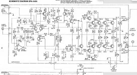
I spent some time today noodling over the bias control circuit of the 545 amp.
Adcom has a tendency to draw their diagrams rather badly, especially right where the input stage meets the output stage (remember in the 565, this is where that messy bias control circuit is).
Here is the bias circuit of the 545 redrawn. As you can see, the capacitor C611 just passes the signal through from Q614 to Q622, while shielding Q622 from the bias point of Q620 (the collector of Q614).

Q616 is a current source who's current is set by the two diodes in the base circuit. It appears that the current here is about 9.7 mA.
The real party occurs with the little trio of resistors (two resistors and a pot) and Q618.
Because the base emitter voltage of Q618 is always 0.7 volts (nominally), the current through the 681 Ohm resistor (R646) is always about 1 mA. Assuming the base current in Q618 is negligible, this means that the current in the resistor stack is also always about 1 mA. And this means that as the value of the pot changes, the voltage drop across the stack will change. So, when the pot is at zero, the drop across the resistor stack will be .001(1820+681)=2.5 volts, and when the pot is at max, the drop will be .001(2200+1820+681)=4.7 volts.
It also means that the current in Q618 is always fixed as well. Since the voltage drop across R646 (the 681 ohm resistor is the same, and the current through Q618 is constant, that means that the base current in Q618 is also constant, even if the resistance of the pot changes. to accommodate that, the voltage at the collector of Q614 must change as the pot resistance changes. And as the overall equivalent resistance of the resistor stack and Q618 change, the voltage at the collector of Q616 must also change (to keep the current constant).
Exactly how they change is not completely clear to me because the current flow through Q618 and the resistor stack are interdependent.
Adcom has a tendency to draw their diagrams rather badly, especially right where the input stage meets the output stage (remember in the 565, this is where that messy bias control circuit is).
Here is the bias circuit of the 545 redrawn. As you can see, the capacitor C611 just passes the signal through from Q614 to Q622, while shielding Q622 from the bias point of Q620 (the collector of Q614).
Q616 is a current source who's current is set by the two diodes in the base circuit. It appears that the current here is about 9.7 mA.
The real party occurs with the little trio of resistors (two resistors and a pot) and Q618.
Because the base emitter voltage of Q618 is always 0.7 volts (nominally), the current through the 681 Ohm resistor (R646) is always about 1 mA. Assuming the base current in Q618 is negligible, this means that the current in the resistor stack is also always about 1 mA. And this means that as the value of the pot changes, the voltage drop across the stack will change. So, when the pot is at zero, the drop across the resistor stack will be .001(1820+681)=2.5 volts, and when the pot is at max, the drop will be .001(2200+1820+681)=4.7 volts.
It also means that the current in Q618 is always fixed as well. Since the voltage drop across R646 (the 681 ohm resistor is the same, and the current through Q618 is constant, that means that the base current in Q618 is also constant, even if the resistance of the pot changes. to accommodate that, the voltage at the collector of Q614 must change as the pot resistance changes. And as the overall equivalent resistance of the resistor stack and Q618 change, the voltage at the collector of Q616 must also change (to keep the current constant).
Exactly how they change is not completely clear to me because the current flow through Q618 and the resistor stack are interdependent.
Last edited:
Prof:
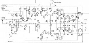
I would suggest looking at the joined left channel schematic I posted above. it has the nominal voltage values in it, so you should be able to determine where in the circuit things are going off.
For example, it shows that in a correctly balanced circuit, the input to R648 and R650 should be 1.7 and -1.7 volts respectively. If that is not the case, then the problem is upstream.
Also, do you have a big 8 ohm resistor? You will need one to properly test the amp. This is what I use.
https://www.mouser.com/ProductDetail/Vishay/RBEF03008R000KFB00?qs=sGAEpiMZZMvKNHcrmI%252BvDeJyIHQjIY4186Qspy2F4Pw%3D
Thanks to you, I have quite a few things lined up.
I am replacing as many of the suspect characters as I can; the previous owner/tech had "tweaked" much, with the result that the amp was running with a high DC offset when I had acquired it. I tried restoring it to the original circuit values.
Use of caps like C611 as a bias voltage 'stabilizer'/hash filter/bypass is quite common in AB amp circuits as far as I know.
Two points:
1) my experience with previous owners is that many of them just fart around trying stuff and in the process end up making things worse. My first 565 had all manner of weird "fixes" that I had to undo before I could even start to get a handle on what was wrong with the amp. So, putting it back to original is a good place to start. Check for leaking electrolytic caps, cold slider joints, fried traces, burnt resistors, etc. I use a nice LED magnifying lamp to inspect the boards and the parts.
2) Caps C611/C612 are not bypass or filter caps, they are coupling caps. they pass the audio signal from one circuit to another while shielding the two circuits from their different DC bias points. If one of them is leaking (as in it has some finite resistance at DC), that will throw off the bias circuit. Probably unlikely, but something to check by lifting one lead and testing its resistance.
Last edited:
No exaggeration, but this thread is the best learning experience I have had. ..
I am checking /replacing stuff systematically, including all the electrolytics.
A funny thing I had noticed in the meantime was that often if a speaker is left connected while powering up, the offset swings to a few volts negative, and comes down a volt or so, but never near say, less than 50 mV. But if you try powering up once again without the speaker connected, then the swing is momentary and corrects in a matter of seconds, and all is normal. Very weird indeed...
All the more reason for me to think that the amp could do with a redesign/mod, so that the wacky servo is replaced by a tried and tested LTP that ought to be stable and more predictable.
Thanks and warm regards
I suspect it depends on the speaker. Speaker crossovers have a bunch of reactive components (inductors and capacitors), and they will react differently to DC. The question is, why is there DC at start up?
I'd try disconnecting and shorting the inputs of R647 and R649. This should shut down the output stages. If there is still an offset, then there is something wrong in the output stage. That is usually either a failed transistor, or a failed emitter stabilizing resistor. These are usually low value base resistors (10 ohms) or very low value emitter resistors (0.22 Ohms 2 watt) intended to provide some feedback for thermal drift.
I'd try disconnecting and shorting the inputs of R647 and R649. This should shut down the output stages. If there is still an offset, then there is something wrong in the output stage. That is usually either a failed transistor, or a failed emitter stabilizing resistor. These are usually low value base resistors (10 ohms) or very low value emitter resistors (0.22 Ohms 2 watt) intended to provide some feedback for thermal drift.
- Home
- Amplifiers
- Solid State
- Yet Another Adcom GFA-565 Thread