Also there are examples where we have introduced
a proprietary local feedback which runs the front end at lower open loop gain.

Do you refer there to CLF (Cascode Local Feedback) in your Xs-amps?
Going through my old notes, the OL gain of the front end is in the high 30's of dB,
...
Also there are examples where we have introduced
a proprietary local feedback which runs the front end at lower open loop gain.
Now you are really piling it on with additional mysterious circuits.
I experimented with some local/global feedback mixes but haven't found anything that improves performance in simulations.
One of these days I need to build the boards and play around on the bench.Now you are really piling it on with additional mysterious circuits.
I experimented with some local/global feedback mixes but haven't found anything that improves performance in simulations.
To me it has always been about what you hear. Glad you are going forward !!!!
To me it has always been about what you hear. Glad you are going forward !!!!
Sometimes I am not sure which direction I am going.
Schematics..
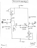
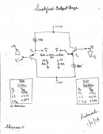
The left image shows the schematic of the output stage of the prototype balanced SE amp. Noteworthy are the following:
1. Each branch idles at a stable 0.3A; because of the high stability of the 1.25 Vdc reference in the voltage regulators, and the relatively small size of the heatsink.
2. The complementary Fairchild power bjts have a disclosed hfe~200; easy to drive with the dual Op Amps [OA] of NE5532.
3. The idle dc voltage at the emitter of PNP is always higher than at the emitter of NPN. For example; ground the bases of bjts. NPN is ~0.7 Vdc [ its Vbe] below common, and PNP is ~0.7Vdc above it. Thus the load Zl [8 Ohm] is coupled by capacitor of shown required polarity [option 1].
4. Loop feedback [if chosen] around both Op Amps of NE5532 originates at the emitters of bjts. This approach allows the idle DC voltage at the bjt emitters to settle at ~0 Vdc, and thus enables the load to be directly connected between the emitters as in option 2.
5. A Zobel [at the emitter of PNP] is required to prevent oscillation in the final amp.
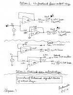
The right image shows two schematics of the generators of balanced input signals, and simultaneous drivers of the power bjts in the left image.
1. The top schematic shows that input signal Vi is presented simultaneously to non-inverting OA1 [voltage gain of +1], and inverting OA2 of voltage gain of -1. Their idle Vout sits at ~0 VDC; which requires using Option 1 to connect the loudspeaker [or Zl] as noted above because of the 1.4 VDC inter emitter offset.
2. The bottom schematic allows for negative feedback in addition to the attributes of the top schematic. Ceramic capacitors [22 pF] must be connected between the output and inverting ports to prevent oscillation. The idle DC at the bjt emitters is ~0V and thus enables direct coupling of the load Zl. The photos of the amp in the previous post used this option 2.
This amp is stable thermally, and against oscillation when using both options to connect a dummy resistor load or a loudspeaker.
Coming up are objective measurements of this amp [option 2] in the form of scope photos which I hope will clearly describe its operation. I do not have the technical capability/equipment to SIM and measure THD.
Best regards.
The left image shows the schematic of the output stage of the prototype balanced SE amp. Noteworthy are the following:
1. Each branch idles at a stable 0.3A; because of the high stability of the 1.25 Vdc reference in the voltage regulators, and the relatively small size of the heatsink.
2. The complementary Fairchild power bjts have a disclosed hfe~200; easy to drive with the dual Op Amps [OA] of NE5532.
3. The idle dc voltage at the emitter of PNP is always higher than at the emitter of NPN. For example; ground the bases of bjts. NPN is ~0.7 Vdc [ its Vbe] below common, and PNP is ~0.7Vdc above it. Thus the load Zl [8 Ohm] is coupled by capacitor of shown required polarity [option 1].
4. Loop feedback [if chosen] around both Op Amps of NE5532 originates at the emitters of bjts. This approach allows the idle DC voltage at the bjt emitters to settle at ~0 Vdc, and thus enables the load to be directly connected between the emitters as in option 2.
5. A Zobel [at the emitter of PNP] is required to prevent oscillation in the final amp.
The right image shows two schematics of the generators of balanced input signals, and simultaneous drivers of the power bjts in the left image.
1. The top schematic shows that input signal Vi is presented simultaneously to non-inverting OA1 [voltage gain of +1], and inverting OA2 of voltage gain of -1. Their idle Vout sits at ~0 VDC; which requires using Option 1 to connect the loudspeaker [or Zl] as noted above because of the 1.4 VDC inter emitter offset.
2. The bottom schematic allows for negative feedback in addition to the attributes of the top schematic. Ceramic capacitors [22 pF] must be connected between the output and inverting ports to prevent oscillation. The idle DC at the bjt emitters is ~0V and thus enables direct coupling of the load Zl. The photos of the amp in the previous post used this option 2.
This amp is stable thermally, and against oscillation when using both options to connect a dummy resistor load or a loudspeaker.
Coming up are objective measurements of this amp [option 2] in the form of scope photos which I hope will clearly describe its operation. I do not have the technical capability/equipment to SIM and measure THD.
Best regards.
Attachments
The stream of data..
In post#135, the output stage of the bridged anti-phase single ended amp was noted to process [or amplify] the positive-going part of a sine wave [for example] differently from its negative-going component. The forthcoming posts beginning with this one will methodically show this unique mode of operation.
I have a Precision Rectifier which takes in a sine wave [20 KHz for this test] and outputs electrically separated positive-going and negative going analog pulses ; which are then used as a diagnostic tool to meet the objective. The resulting positive or negative-going analog pulse train is then input to the generator of balanced signals and simultaneous driver of the output stage [option 2] as if it is a train of sine or music signals.
Each upcoming post like this one will show a simplified schematic of the output stage, and scope photos which describe or show its power output signals; be it analog pulse like this one or sine.
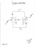
The simplified schematic of the output stage in the left image shows the following:
1. A positive-going analog pulse [train] at base of NPN
2. A balanced negative-going analog pulse [train] at the base of PNP.
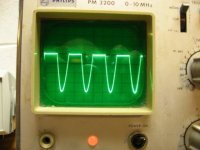
3. The left scope photo describes/shows the power output at the emitter of NPN [Va] for/at each of the indicated loads; NL =no load, balanced [Bal], and dual Single Ended [SE].
4.Similarly, the right scope photo describes the output at the emitter of PNP uner the same load conditions.
5. I imposed a +/- 4 Vpeak at Va and Vb respectively to safeguard the components under load; in the balanced and in the dual SE modes. I readily, and briefly pushed +/-Vp to higher levels and to the eventual clipping for either side. No problems in pushing higher power outputs.
It follows that the "action" at the power outputs were solely determined by/attributed to an increased and simultaneous current conduction of the bjts through the loads. The CCSs played the sole and important role of connecting the emitters to the PSU rails, and had no role in amplifying the positive-going portion//component of sine as simulated by the positive-going pulse train.
Next up is the equally important post describing the operation of the output stage with input negative and positive pulses at NPN and PNP respectively; namely the opposite state to the above.
In post#135, the output stage of the bridged anti-phase single ended amp was noted to process [or amplify] the positive-going part of a sine wave [for example] differently from its negative-going component. The forthcoming posts beginning with this one will methodically show this unique mode of operation.
I have a Precision Rectifier which takes in a sine wave [20 KHz for this test] and outputs electrically separated positive-going and negative going analog pulses ; which are then used as a diagnostic tool to meet the objective. The resulting positive or negative-going analog pulse train is then input to the generator of balanced signals and simultaneous driver of the output stage [option 2] as if it is a train of sine or music signals.
Each upcoming post like this one will show a simplified schematic of the output stage, and scope photos which describe or show its power output signals; be it analog pulse like this one or sine.
The simplified schematic of the output stage in the left image shows the following:
1. A positive-going analog pulse [train] at base of NPN
2. A balanced negative-going analog pulse [train] at the base of PNP.
3. The left scope photo describes/shows the power output at the emitter of NPN [Va] for/at each of the indicated loads; NL =no load, balanced [Bal], and dual Single Ended [SE].
4.Similarly, the right scope photo describes the output at the emitter of PNP uner the same load conditions.
5. I imposed a +/- 4 Vpeak at Va and Vb respectively to safeguard the components under load; in the balanced and in the dual SE modes. I readily, and briefly pushed +/-Vp to higher levels and to the eventual clipping for either side. No problems in pushing higher power outputs.
It follows that the "action" at the power outputs were solely determined by/attributed to an increased and simultaneous current conduction of the bjts through the loads. The CCSs played the sole and important role of connecting the emitters to the PSU rails, and had no role in amplifying the positive-going portion//component of sine as simulated by the positive-going pulse train.
Next up is the equally important post describing the operation of the output stage with input negative and positive pulses at NPN and PNP respectively; namely the opposite state to the above.
Attachments
I reran the damping factor calculations for my LTSpice simulation of a XA30.8-Guess using Bob Cordell's subthreshold VDMOS Spice models for the IRFP240 and IRFP9240 FETs http://www.diyaudio.com/forums/soft...-power-mosfet-models-ltspice.html#post4158594. With only 10dB of feedback I got a damping factor of 59 rather than the 150 on the Pass Labs spec sheet. Thus I need about 18dB feedback in my circuit to get to a damping factor of 150. My bench measurements of those FETs at 300mA agrees fairly well with the new Spice models.
Hello lhquam,
thank you for the great link. With the new models my simulation results now look less misterious and more what I would expect. I am working on solving the rest.
Regarding your capacitor trick I found it helpful to even increase the value from 1000µF to 1F. 1000µF still influenced the simulation results.
The image shows a simplified schematic for the output stage of the balanced SE amp [under test] which is a prototype of the bridged anti-phase single ended amp taught by lhquam. It is the companion schematic to that shown in post #188 with the important difference of reversed input analog pulse signals to the bases of bjts. This arrangement of input signals has an important consequence which is to decrease the conduction of current in the bjts and cut them off in the limit.
For the sake of simplicity/clarity, the scope photos are taken only at the emitter of PNP [Vb=power output]. The tracking scope photos at emitter of NPN are inverted [not shown] and have identical behavior or looks.
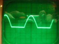
The pair of scope photos which show a tall clean and a tall distorted positive-going pulses pertain to operating the output stage in a dual SE mode.
1. The peak voltage across 8 Ohm resistor is 2.3 V [for clean pulse] which translates to ~0.3A; meaning the current level sourced by LM337.
2. The companion tall and distorted pulse was induced by increasing slightly the input pulse signal. Why the distortion? PNP cut off, and has effectively donated fully its idle current [0.3 A] to the load.
3. It is apparent that in between the state of idle and of peak power delivery, PNP and LM337 were simultaneously contributing to output power; which is different from that observed in the operation of the output stage in post #188; namely the sole power output contribution by bjts.
4. The box at the bottom left of the schematic shows data relating Vbe [measured base-emitter voltage ] of PNP with/at its idle, at Vp clean, and at Vp distorted. The distorted Vp state induced cut off in PNP [Vbe ~0.37 V]. It ran out of current.
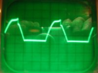
The pair of scope photos showing short clean and distorted pulses pertain to operating the output stage in bridge mode.
1. The amplitude of the clean pulse is ~1.2 Vp
2. Together with the companion inverted pulse at emitter of NPN gives a Vpeak to peak of 2.4 V across 8 Ohms to yield 0.3 A which is the maximum offering by each CCS.
3. The distorted short pulse signal was induced by slightly increasing the input signal to the base of PNP.
4. The data in the box on the right of the schematic show that PNP experienced cut off [Vbe ~0.35V] at this condition of distorted pulse output.
5. Again, the a clean power output of the amp was limited by the preset idle current of the CCSs; unlike that in post#188 [its V peak to peak was 8 V across 8 ohms to afford 1 A which was limited [by me] only by the size of heat sink, base drive, Vce of bjts, PSU capability, SOA, etc..]
6. I hope it is clear to see the asymmetric operation of this output stage ~unlimited power output in one direction of the input sine signal, and a restrained or limited power output in the other/opposite direction of the input sine signal.
It follows that the Vp-p of a clean sine signal [20 KHz] across 8 Ohms will have the value of a maximum 4.8 V [pushing 0.6 Ap-p]. An only 0.3A contribution comes from the "unlimited" performance, and a maximum 0.3 A comes from the limited performance. Will show this.
For the sake of simplicity/clarity, the scope photos are taken only at the emitter of PNP [Vb=power output]. The tracking scope photos at emitter of NPN are inverted [not shown] and have identical behavior or looks.
The pair of scope photos which show a tall clean and a tall distorted positive-going pulses pertain to operating the output stage in a dual SE mode.
1. The peak voltage across 8 Ohm resistor is 2.3 V [for clean pulse] which translates to ~0.3A; meaning the current level sourced by LM337.
2. The companion tall and distorted pulse was induced by increasing slightly the input pulse signal. Why the distortion? PNP cut off, and has effectively donated fully its idle current [0.3 A] to the load.
3. It is apparent that in between the state of idle and of peak power delivery, PNP and LM337 were simultaneously contributing to output power; which is different from that observed in the operation of the output stage in post #188; namely the sole power output contribution by bjts.
4. The box at the bottom left of the schematic shows data relating Vbe [measured base-emitter voltage ] of PNP with/at its idle, at Vp clean, and at Vp distorted. The distorted Vp state induced cut off in PNP [Vbe ~0.37 V]. It ran out of current.
The pair of scope photos showing short clean and distorted pulses pertain to operating the output stage in bridge mode.
1. The amplitude of the clean pulse is ~1.2 Vp
2. Together with the companion inverted pulse at emitter of NPN gives a Vpeak to peak of 2.4 V across 8 Ohms to yield 0.3 A which is the maximum offering by each CCS.
3. The distorted short pulse signal was induced by slightly increasing the input signal to the base of PNP.
4. The data in the box on the right of the schematic show that PNP experienced cut off [Vbe ~0.35V] at this condition of distorted pulse output.
5. Again, the a clean power output of the amp was limited by the preset idle current of the CCSs; unlike that in post#188 [its V peak to peak was 8 V across 8 ohms to afford 1 A which was limited [by me] only by the size of heat sink, base drive, Vce of bjts, PSU capability, SOA, etc..]
6. I hope it is clear to see the asymmetric operation of this output stage ~unlimited power output in one direction of the input sine signal, and a restrained or limited power output in the other/opposite direction of the input sine signal.
It follows that the Vp-p of a clean sine signal [20 KHz] across 8 Ohms will have the value of a maximum 4.8 V [pushing 0.6 Ap-p]. An only 0.3A contribution comes from the "unlimited" performance, and a maximum 0.3 A comes from the limited performance. Will show this.
Attachments
Feedback Loops
Trying to unravel the secrets of the XA.8 has been a stimulating exercise for me, which thru many experiments has been a learning experience. Bridged and push-pull amplifiers have so much even harmonic cancellation that it is difficult to obtain a high H2/H3 ratio. Global feedback negates the effects of introducing H2 in the output stage via. manipulating the NFET/PFET transconductances via the introduction of SE bias current.
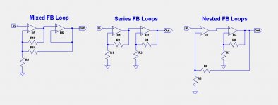
The hint about local feedback in Nelson's recent post http://www.diyaudio.com/forums/pass...gle-ended-current-sources-18.html#post4182080 put my on a new path. I experimented with summing feedback currents from the final outputs and the front-end outputs into the jfet source nodes. That shows some promise, but it became apparent that either nested or series feedback loops might do much better. With the topology of the X.8 how can two loops be devised?
With series loops, the first loop can establish a high H2/H3 ratio and then the second loop uses feedback to conform to the output of the first loop. But that approach is in conflict with the XA.8 output stage having a high H2 signature which we do not want to cancel.
With nested loops it is harder to understand how to make it work. The outer loop closes from the amplifier outputs to the and the inputs. The inner loop involves the front-end outputs into the output-stage feeding back to somewhere, but where?
So the question remains: How to have a high H2/H3 ratio from the output stage without feedback cancellation, and also achieving 150-200 damping factor?
Trying to unravel the secrets of the XA.8 has been a stimulating exercise for me, which thru many experiments has been a learning experience. Bridged and push-pull amplifiers have so much even harmonic cancellation that it is difficult to obtain a high H2/H3 ratio. Global feedback negates the effects of introducing H2 in the output stage via. manipulating the NFET/PFET transconductances via the introduction of SE bias current.
The hint about local feedback in Nelson's recent post http://www.diyaudio.com/forums/pass...gle-ended-current-sources-18.html#post4182080 put my on a new path. I experimented with summing feedback currents from the final outputs and the front-end outputs into the jfet source nodes. That shows some promise, but it became apparent that either nested or series feedback loops might do much better. With the topology of the X.8 how can two loops be devised?
With series loops, the first loop can establish a high H2/H3 ratio and then the second loop uses feedback to conform to the output of the first loop. But that approach is in conflict with the XA.8 output stage having a high H2 signature which we do not want to cancel.
With nested loops it is harder to understand how to make it work. The outer loop closes from the amplifier outputs to the and the inputs. The inner loop involves the front-end outputs into the output-stage feeding back to somewhere, but where?
So the question remains: How to have a high H2/H3 ratio from the output stage without feedback cancellation, and also achieving 150-200 damping factor?
Attachments
Last edited:
Is the "hawksford cascode" a form of localized feedback? Thinking on the F3 and how the cascode device was used as a tool of manipulation.
I am not sure if the Hawksford Cascode should be considered feedback or error correction.
Ok. What of F3 style feedback to cascode.
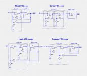
The F3 cascode modulation is optimized for the properties of the power JFET used. The Hawksford cascode would probably help the performance, but is unlikely to help with the problem of H2 cancellation. We are looking for a way to preserve H2 while reducing H3 without excessive feedback. Alternatively, if the output stage has low enough output resistance to maintain a high damping factor, we can use a very low amount of global feedback and minimize H3 in the front-end feedback loop. That approach would be one of the left column feedback schemes in post #192 (Mixed or Nested FB Loops).
are we sure that the output stage is included in the feedback loop. In the past it seems it was suggested that the output stage was operated open loop
With the bigger amps with more FETs, the output resistance would be low enough to get a high damping factor without being in the feedback loop. With the XA30.8 and only 20 FETs per channel, the output resistance is too high without a bit of negative feedback.
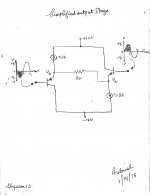
The image shows a simplified schematic of the balanced SE amp which is a bjt prototype of lhquam's bridged anti-phase single ended amp. Please mnote:
1.The input sine signals are 180 degrees out of phase as prescribed by lhquam.
2. The power output signals at Va [NPN], and Vb [PNP] are not shown. They are like [in phase and amplitude] their respective input signals since the bjts operate in the common collector configuration.
3. Let's focus on the left SE branch [PNP], and note its input sine signal. The discussion holds equally well to the right SE branch. My hand drawing of it is imperfect. The shaded [negative-going], and clear components were meant to have identical Vp, and areas under their curves.
4. During the time interval spanning 0 to t seconds, PNP idles at 0.3 A at 0 and t seconds. One may wish to mentally erase or white-out the clear component [t to t1] because it is not there yet.
5. This resultant snapshot is identical to that shown in post #188, and its scope photos.
6. During the time interval of t to t1 seconds, one may as well erase/white out mentally the shaded component of the sine signal because it is akready gone.
7. The resultant snapshot is identical to that of post#190 and its scope photos.
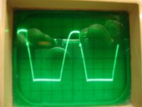
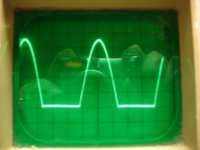
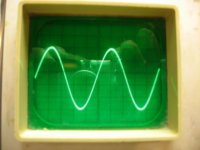
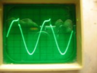
8. The left clean-looking scope photo pertains to PNP at Vb. It has a peak to peak voltage amplitude of ~2.5V relative to common. There is another one like it at NPN [Va]; but is 180 degrees out of phase. [Homework..Calculate maximum rms power output in 8 Ohms].
9.The distorted signal at Vb in the right scope photo emanated when the input sine signal was increased slightly. There is an inverted one like it at Va. This is a gross, and blatant distortion; akin to clipping [signal eventually becomes square] because of the CCSs limited offering of 0.3A each, and/or the consequent cutoff of the bjts.
10. It follows that the pleasing harmonic distortion of this amp is/can only be buried in its performance depicted by the clean-looking scope photo and absolutely not that of or due the distorted one..
I will repeat this current test by using Option 1 [capacitor-coupled load] which will not use negative feedback from the power outputs [Va and Vb] to the Op Amp inverting inputs. It follows that I will have two options to listen to its performance in bridged anti-phase SE mode; with and without negative feedback.
1.The input sine signals are 180 degrees out of phase as prescribed by lhquam.
2. The power output signals at Va [NPN], and Vb [PNP] are not shown. They are like [in phase and amplitude] their respective input signals since the bjts operate in the common collector configuration.
3. Let's focus on the left SE branch [PNP], and note its input sine signal. The discussion holds equally well to the right SE branch. My hand drawing of it is imperfect. The shaded [negative-going], and clear components were meant to have identical Vp, and areas under their curves.
4. During the time interval spanning 0 to t seconds, PNP idles at 0.3 A at 0 and t seconds. One may wish to mentally erase or white-out the clear component [t to t1] because it is not there yet.
5. This resultant snapshot is identical to that shown in post #188, and its scope photos.
6. During the time interval of t to t1 seconds, one may as well erase/white out mentally the shaded component of the sine signal because it is akready gone.
7. The resultant snapshot is identical to that of post#190 and its scope photos.
8. The left clean-looking scope photo pertains to PNP at Vb. It has a peak to peak voltage amplitude of ~2.5V relative to common. There is another one like it at NPN [Va]; but is 180 degrees out of phase. [Homework..Calculate maximum rms power output in 8 Ohms].
9.The distorted signal at Vb in the right scope photo emanated when the input sine signal was increased slightly. There is an inverted one like it at Va. This is a gross, and blatant distortion; akin to clipping [signal eventually becomes square] because of the CCSs limited offering of 0.3A each, and/or the consequent cutoff of the bjts.
10. It follows that the pleasing harmonic distortion of this amp is/can only be buried in its performance depicted by the clean-looking scope photo and absolutely not that of or due the distorted one..
I will repeat this current test by using Option 1 [capacitor-coupled load] which will not use negative feedback from the power outputs [Va and Vb] to the Op Amp inverting inputs. It follows that I will have two options to listen to its performance in bridged anti-phase SE mode; with and without negative feedback.
Attachments
are we sure that the output stage is included in the feedback loop. In the past it seems it was suggested that the output stage was operated open loop
AFAIK later models have included OS into feedback loop. In older models up from X600 OS was not included.
- Status
- This old topic is closed. If you want to reopen this topic, contact a moderator using the "Report Post" button.
- Home
- Amplifiers
- Pass Labs
- XA.8 single-ended current sources