I got the LA issue and FETs today.
LSK170: Idss = 12 mA, Yfs = 39 mS
LSJ74: Idss = 8.4 mA, Yfs = 30 mS
Can you show us the curves?
Like the Toshibas the LT devices are symmetrical in the sense that gate and source can be inverted giving identical traces.
The (one) LSK170 I got is similar to my 2SK170's in terms of Idss/Yfs, but I did not look at the actual traces yet.
The (one) LSJ74 I have is very different from my 2SJ74 having about half the transconductance.
Maybe degeneration of the LSK170 (or 2SK170) will result in better complementarity with the LSJ74.
Difficult to say with one of each of the LTs
IMO the "average" device is of little interest as one of the (few) advantages of DIY is that we don't have to worry about the average and can go for the perfect match
Yes - later.
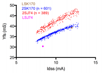
I have attached a graph showing how they compare to my stash of Toshibas in terms of Idss and Yfs.
Great, this is the way to present the data. Notice how tight the N distribution is compared to the P.
The easiest method I've seen is glue-and-paste, followed by time under the salamander grill.I could write an article about SMT soldering for the DIY community, if that is something that you think would be of use to your readership.
The challenge is working out just how long you need under the grill (or IR lamp) for each part and in what order you do them. But it's not that hard with "side" attaching devices.
<old fart>
I remember doing our first multi-hundred connector BGAs - by the time they'd started to attach all the passives had floated away! Even on "pro" gear it took us quite a few attempts goes to get a good, repeatable heat profile.
</old fart>
Yes - later.
I have attached a graph showing how they compare to my stash of Toshibas in terms of Idss and Yfs.
Thanks. Quite interesting. It appears to someone relatively ignorant such as I, that if creating, for example, a LTP with Toshiba's N channel SK170s, that a match for Idss alone would result in a close match to Yfs in the linear range of performance. But not so much with the p channel device. Again, a great plot of data.
Have tweezers, will travel
I don't like playing tiddly winks with SMT parts.
Yes - later.
I have attached a graph showing how they compare to my stash of Toshibas in terms of Idss and Yfs.
Here's a few more samples, from a figure to be used in an upcoming Linear Audio article. 10 of them from a lot sent to me by LS (date code 1213) and 10 sent to me by Jan (no date)- there's really no difference between them, so Jan's lot is probably the same.
Attachments
In all my years doing SMT, I have never used or had to resort to this method. Not to say it won't work and maybe teh only option for certain parts such as BGA conns. Recall doing SMT Berg's which was a paste/insert/reflow op = tricky even for the sub contract mfg.The easiest method I've seen is glue-and-paste, followed by time under the salamander grill.
A hot-air machine is invaluable for SMT removal. The Sparkfun unit functions similar to the Hakko I have used in the past, nozzles are interchangeable.
Back to lsk pch jfets that are in TO-92!! Since now having current production p-ch jfets, I assume that some older/newer symmetrical, push-pull designs will resurface.
And the ramifications are? more distortion? in a push-pull arrangement.The (one) LSJ74 I have is very different from my 2SJ74 having about half the transconductance.
Any spice models for the 2SJ74 yet?
SMD / SMT soldering
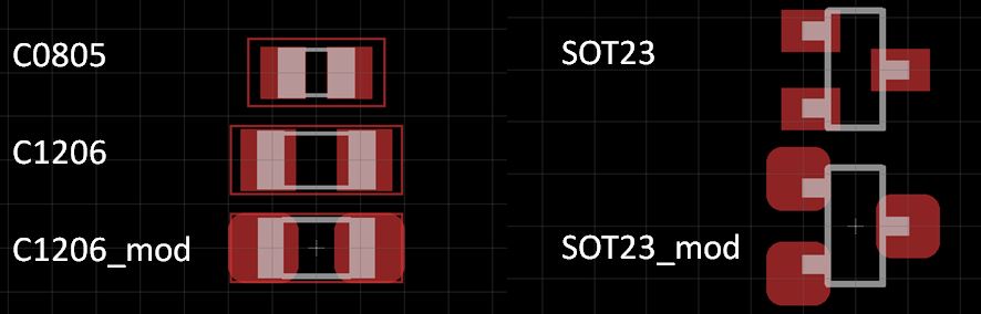
I like to optimize/modify the package footprints in availble libraries for easier hand soldering. I don't have any issues with relatively big, e.g. 1206 packages, but bigger pads are more forgiving against lifting after several solder/desolder steps. Also, 1206 footprints that additionally supports 0805 is often handy.
-- xLoff
Attachments
.model J2sj74 PJF(Beta=92.12m Rs=7.748 Rd=7.748 Betatce=-.5 Lambda=4.464m
+ Vto=-.5428 Vtotc=-2.5m Cgd=85.67p M=.3246 Pb=.3905 Fc=.5
+ Cgs=78.27p Isr=129.8p Nr=2 Is=12.98p N=1 Xti=3 Alpha=10u Vk=100
+ Kf=26.64E-18 Af=1)
model J2sk170 NJF(Beta=59.86m Rs=4.151 Rd=4.151 Betatce=-.5 Lambda=1.923m
+ Vto=-.5024 Vtotc=-2.5m Cgd=20p M=.3805 Pb=.4746 Fc=.5
+ Cgs=25.48p Isr=84.77p Nr=2 Is=8.477p N=1 Xti=3 Alpha=10u Vk=100
+ Kf=111.3E-18 Af=1)
I tripped over these awhile back, if you are looking for spice models...
Regards, E
I think we were wave-soldering mixed SMT (bottom and top mounted) and through hole devices. The BGAs had their own pick/place/solder machine (It was a long time ago).In all my years doing SMT, I have never used or had to resort to this method.
Are the current pastes sticky enough to stop devices moving during DIY heating?
Last edited:
I'm a fan of the combined 0805/1206 footprints where the available PWB acreage isn't forcing 0805 packages. The downside is "you can't route a trace under the part between the pads". This practice is often already against the "house rules" in many places so little is lost by enlarging the 1206 pads.I like to optimize/modify the package footprints in availble libraries for easier hand soldering. I don't have any issues with relatively big, e.g. 1206 packages, but bigger pads are more forgiving against lifting after several solder/desolder steps. Also, 1206 footprints that additionally supports 0805 is often handy.
Enlarging the SOT-23 pads as shown looks like a reasonable modification. Leave enough space between the two pads so a trace can be run between them.
Dale
Do not know for sure but I doubt it, I really have never used paste for hand assembly. I hand bomb them, one pin at a time, use the hot air pencil if I have to remove, re-flow. I do not do any BGA at home, thank god they are sort of standardizing on DFN for most analog/mixed-sig in small pin counts or I'd be toast.Are the current pastes sticky enough to stop devices moving during DIY heating?
It is so expensive to get pcb's soldered up.
Yes I agree, about altering pads for the solder process/application, same as wave (back-side) vs re-flow pads. I usually run the pad exit at the same or larger (neck up/down) than the pad. It is all in the libraries. Stock libraries do not know process? I remember back at HP, they had auto pad/geom generation, based on the smt process selection, lots of ample code overlaying the Mentor Board Station core. The RF/lab/mfg teams knew what they were doing. Not sure where HPDL ended up esp. after the Agilent break.I like to optimize/modify the package footprints in availble libraries for easier hand soldering.
The beauty of hand soldering, is that I can break this rule, "no phone call from the process police" since every solder joint is inspected"you can't route a trace under the part between the pads". This practice is often already against the "house rules"
Gottem, but thanks just the same.if you are looking for spice models...
Rick
"you can't route a trace under the part between the pads". This practice is often already against the "house rules"
I know how you feel about the "process police". In many cases they seem to aggressively enforce rules that have lost their original justification. But this is one rule (no traces running under the parts, between the pads of 1206, 0805, and 0603 packages) that I'm in favor of, even though the basis for the rule is much weaker for hand-soldered boards than for automated SMT assembly.The beauty of hand soldering, is that I can break this rule, "no phone call from the process police" since every solder joint is inspected"you can't route a trace under the part between the pads". This practice is often already against the "house rules"
Dale
Ok,so i get a mail saying
What?When?Where?We are creating a retail outlet for users like you which will be available in 2-3 weeks. Keep checking the diyaudio site for an annoucement
Ok,so i get a mail saying
What?When?Where?
Why do you ask three questions that were answered in the email to you??
- Status
- This old topic is closed. If you want to reopen this topic, contact a moderator using the "Report Post" button.
- Home
- Amplifiers
- Pass Labs
- Will linear deliver on promised lsj74