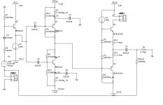
ashade said:look now. I've changed the output state and put Rfeed for feedback.
A slightly different connection will get rid of R8 and I1 as well as improve DC offset. The input stage bias arrangement insures that the output voltage swing is only about +-3.5V or less, so your amp only produces a bit more than 1.5W output before clipping out of the 20W possible from +-15V power rails. This should be easy to improve, though your input stage by necessity limits output swing, unless it has separate higher voltage supplies.
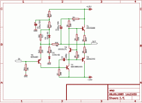
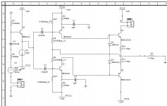
Non differential input DC coupled amp
Let's go for a (conceptual) power amp design, DC coupled with bootstrapped VAS for a +/- 15V power supply. Output DC voltage can be adjusted by changing R14/R10. Bias can be adjusted by replacing R5 by a pot. Output stage should be sufficiant to handle a 4 ohm load. As the VAS stage T4 is biased by nearly 100 ma, it should mounted on a heatsink.
This amp is neither simulated nor build in any way but it should work. Notice that there is not JFET or MOSFET in the circuit, only BJT's. T5 and D1 provides an error reduction circuit, replacing the BJT from a LTP input by a simple diode. R13 is adding an additional current to the feedback summing point, because the feedback potential is about +0.65V not 0V. In this way the output voltage should be near 0V.
Attachments
I've changed the output state and put Rfeed for feedback.
ashade,
your feedback will not work as the feedback summing point at Q3 is a low impedance node (about 40 ohms) and a current change in this node will not result in an output voltage change.
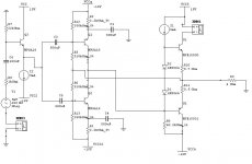
Your input stage bias arrangement puts approximately 7.8V on each emitter resistor. Since the collector cannot swing more than the voltage on the emitter, this is what limits your output voltage - the effective input stage power supply is +-(15-7.8)=+-7.2V. And that is if the transistors have exactly the same beta. The output stage loses one Vbe (0.6V or so) off of that too. These should be sufficient clues for you to figure out what to do.
And while you are at it, you can delete I1 and R8, and put the two diodes in circuit between collectors of Q1 and Q2. You can also connect the junction of R5 and R6 to the output instead of where it is now, which will make the output swing symetrically and also include it's offset in the biassing arrangement and therefore remove it from consideration. Adjust R10 and R11 for desired output stage bias current.
So much for topological limits to output swing. Your feedback arrangement (which BTW will not work well in the real world!) is what limits the actual swing (and also makes R9 quite useless).
So much for topological limits to output swing. Your feedback arrangement (which BTW will not work well in the real world!) is what limits the actual swing (and also makes R9 quite useless).
R9 is the output impedance of the signal source (a mic for example). That's why it's between the cap and the signal source.
Ashade, I cannot comment on everything in this design, but it has many compromises. It is not the way a normal design engineer would use the available components, and it is prone to poor reliability. The output cap is much too low in value, the driver stage should be at a HIGHER voltage than the output stage, etc.
Caps? They are usually expensive, have poor reliability, and cause distortion and phase shift. I hope that this helps
Caps? They are usually expensive, have poor reliability, and cause distortion and phase shift. I hope that this helps
It's 1k does not make much of a difference with 22k in series, but it should be a clue as to why this feedback arrangement is not very good - the gain of the amp depends on the impedance of the source. You are aware that you have 2 feedback loops?
alright, you're saying that the input impedance is getting higher because of Rfeed = 22k. But I've got a book saying that the series-shunt feedback is good for Voltage Amplifiers because it INCREASES the amp input impedance and decreases the amp output impedance. They have a demonstration for it. I really don't understand this.
OK, a few more clues:
Why do R1 and R2 have to be 2.2k?
What is the input impedance of the gain stage?
You still have I1 and R8 in there for really no good reason. Remove them, then remove the connection from Q1 C to Q2 C (keep the connection from Q2 C to U2 B). Then add connection from Q1 C to U1 B. This way the gain stage current is shared with the boas diodes and an extra current source and resistor is not needed. Besides, R8 is additionally loading your gain stage reducing it's gain (and it also intorduces a DC offset)
Regarding the input impedance of the amp and your feedback question, here is a question for you: what determines the input impedance of your amplifier?
Otherwise, you can't have something for nothing. Feedback reduces output impedance and increases input impedance at the expense of lowering gain by the same factor.
You still have I1 and R8 in there for really no good reason. Remove them, then remove the connection from Q1 C to Q2 C (keep the connection from Q2 C to U2 B). Then add connection from Q1 C to U1 B. This way the gain stage current is shared with the boas diodes and an extra current source and resistor is not needed. Besides, R8 is additionally loading your gain stage reducing it's gain (and it also intorduces a DC offset)
I've done what u said but I'm having problems to get Q1 to work on active mode. Its seems it'll be very hard to bias it.
I1 is used to rise the input impedance of the output stage. Without it, the amp gain has tottaly fallen down. With a 100mA current source, the gain is about 1700 times. With no current source, the gain is about 180 times, much lower. That resistor is not useful, so I've revomed it as you said.
Originally posted by ashade
I've done what u said but I'm having problems to get Q1 to work on active mode. Its seems it'll be very hard to bias it.
That is because you have also done things I did not tell you:
1) you removed emitter resistors for Q1 and Q2 - without them you get no biassing stability at all. I did ask you why they were 2.2k - meaning, why not 1k or 4k or 100 ohm? There is a speciffic reason I asked - somewhere in your text books, there is a simple rule about voltage drop across this resistor in order to get good bias stability. Once emitter resistors are back, you still need the capacitors to ground that you have also removed.
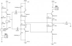
2) Your bias diodes for output stage have no current going through them meanin the top transistor (U1) is not biassed into the active region, hence output offset. U1 base still has to go to Q1 collector. The total circuit there is: Q1 C to U1 B and D1 A, D1 K to D2 A, D2 K to U2 B and Q2 C.
ashade said:I1 is used to rise the input impedance of the output stage. Without it, the amp gain has tottaly fallen down. With a 100mA current source, the gain is about 1700 times. With no current source, the gain is about 180 times, much lower. That resistor is not useful, so I've removed it as you said.
You cannot rise impedance of the output stage by putting in parallel with it's input a current source. This is basic electricity - your output stage has an input impedance and you have put the infinite impedance of the current source in parallel with it for AC. X ohms in parallel with infinity is still X ohms. The reason you get no gain is because you get no bias current through U1 and U2, because U1 gets no base current, because there is no current through D1 and D2, in other words the circuit DOES NOT WORK as an amplifier.
You still have not answered two questions I asked:
1) What is the input impedance of the gain stage
2) What is the input impedance of the whole amplifier
These are very simple qquestions and for your amplifier, the answers are in both cases determined by one single component, respectively.
Until you answer this, I cannot further help you because you will not understand what I am telling you.
for the whole amp, input impedance is only dependent on MPSA18 bias. IC~3mA and Bf=2.56k; therefore, input impedance = 2560 * 25.8e-3 / 3e-3 ~ 22kOhm.
for the gain state I admit I don't know how to calculate because of the feedback.
alright, Ill do it. But I've never seen this output state this way... at least in my books. Could you explain me how it works for large ac signals?
for the gain state I admit I don't know how to calculate because of the feedback.
Your bias diodes for output stage have no current going through them meanin the top transistor (U1) is not biassed into the active region, hence output offset. U1 base still has to go to Q1 collector. The total circuit there is: Q1 C to U1 B and D1 A, D1 K to D2 A, D2 K to U2 B and Q2 C.
alright, Ill do it. But I've never seen this output state this way... at least in my books. Could you explain me how it works for large ac signals?
You have a rather obvious error - Q1 cannot be MPSA18 because it has to be PNP, and Vccg must be +15V not -15V (again, this is basic stuff). Don't know off-hand what the complementary of a MPSA18 is. You could try BC337, BC327 in the gain stage... or BC546, BC556.
DC input resistance of your whole amplifier is equal to R7. This is because your follower is loaded by a current source which has infinite impedance. From the input (base) the impedance equals hie of Q3 plus whatever impedance is on the emitter times (beta + 1). Since the latter is infinity, infinity times anything equals infinity, plus anything still equals infinity. 22k in parallel with that equals 22k.
AC input impedance depends entirely on R7 and the input impedance of the gain stage, biassing of your gain stage. In effect the latter is hie of Q1 in parallel with Hie of Q2, hie is approximately 0.025/Ib, Ib assuming equal beta of Q1 and Q2 is roughly (((15V * 330)/(330 + 200))-0.6)/((beta + 1)*1k). Depending on beta it comes out on the order of 150-450 ohms. R5, 6, 12 and 13 end up being far larger than that regardless of feedback and can safely be disregarded. Once you multiply this with (beta+1) of Q3 and add hie of Q3, you get about 15-135k(depending on all the betas) in parallel with R7. It comes out as 9.7 to 18.9k, for beta is between 100 and 300.
DC input resistance of your whole amplifier is equal to R7. This is because your follower is loaded by a current source which has infinite impedance. From the input (base) the impedance equals hie of Q3 plus whatever impedance is on the emitter times (beta + 1). Since the latter is infinity, infinity times anything equals infinity, plus anything still equals infinity. 22k in parallel with that equals 22k.
DC input resistance isn't calculated replacing the bjt by a small signal model, right?
AC input impedance depends entirely on R7 and the input impedance of the gain stage,
if you replace by the T model, neglecting Early effect, you can see that the input impedance depends also on Re = Vt/Ie ~ 8.6Ohm. This is very low. However, we'll have: Rin = Rb // (Bf+1)(RL+Re) ~ (Bf+1)*RL, because Rb is very large.
- Status
- This old topic is closed. If you want to reopen this topic, contact a moderator using the "Report Post" button.
- Home
- Amplifiers
- Solid State
- Why always differential stages?