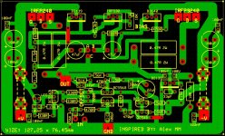
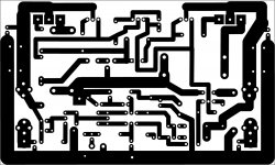
Attempt for PCB
Inspired by Alex MM and his pieces of art PCB's I decide to try to create one for this project because this actually is my amp that I listen every day and enjoying its very good sound. Now is build on veroboard and I think it deserves a PCB. Some day will rebuild it totally with nice PCB's better heatsink and better box.
Attaching the schematic and PCB top and B&W images.
On the PCB and on the schematic there are tree link points - A , B and C.
Previous in the thread I was suggested to move the bootstrap source from output to the emitter of the BD139 driver transistor. I did not try this yet but made the PCB to be able to try it. If you link A and C points source will be at the output and if you link A and C points source will be at the emitter of BD139 driver. So you will be able to change the source according to your taste")
Be Happy!
Inspired by Alex MM and his pieces of art PCB's I decide to try to create one for this project because this actually is my amp that I listen every day and enjoying its very good sound. Now is build on veroboard and I think it deserves a PCB. Some day will rebuild it totally with nice PCB's better heatsink and better box.
Attaching the schematic and PCB top and B&W images.
On the PCB and on the schematic there are tree link points - A , B and C.
Previous in the thread I was suggested to move the bootstrap source from output to the emitter of the BD139 driver transistor. I did not try this yet but made the PCB to be able to try it. If you link A and C points source will be at the output and if you link A and C points source will be at the emitter of BD139 driver. So you will be able to change the source according to your taste
Be Happy!
Attachments
Last edited:
Like that you won't be able to twist the supply leads together.
What do you mean with that? Can't twist supply wires together which is possible or what? On the PCB there is no output GND it is taken directly from the power supply. Amplifier work like this now and it is dead silent - if you put your ear to the speaker you won't understand whatever amp is turned ON or is OFF.
By twisting the supply leads with ground you magnetically couple them so the magnetic fields cancel and don't radiate into nearby circuits.
The power traces as they are now form a big loop around the PCB, radiating into everything inside. At significant currents these are highly distorted rectified waves. Look at how OStripper did the DIYAmp PCB:
http://www.diyaudio.com/forums/soli...amp-class-ab-amp-diyaudio-11.html#post2894720
That may give you some inspiration. If you can keep the power/ground lines close and twist them together (or perhaps better just to heatshrink them into an untwisted triangle; for a more uniform magnetic field and close coupling), there will not be so much inductance between the board and the offboard large lytic caps, again reducing EMI.
Unfortunately the nice symmetry is lost. Bummer.
Unfortunately I don't have signal generator can use PC for that but just to 17-18KHz and it is not enough I think. Maybe is a time to make myself one.
The big problem is that also I don't have oscilloscope and can't make myself one and of course it costs money which are a bit problematic now for me. I really really want one but can't afford at the moment
can use PC for that but just to 17-18KHz and it is not enough I think. Maybe is a time to make myself one.The big problem is that also I don't have oscilloscope and can't make myself one and of course it costs money which are a bit problematic now for me. I really really want one but can't afford at the moment
Here is a simple, balanced, battery powered square wave generator capable of very fast risetimes with good transistors. It might not be very useful without a scope, but it beats paying hundreds of $ for a signal generator with reasonable risetimes. Transistors should be fast, low-capacitance, low-current types like the PN2369A, 2N5769, 2N5771... Output voltage is only +-.6V but maybe that could be improved...
It could be adapted for triangle wave output with variable symmetry, and the triangle could be shaped into a sine wave, though it would not be a short project.
http://www.diyaudio.com/forums/soli...as-lateral-output-perfect-44.html#post2773967
Perhaps you could build a sampler and use that with your soundcard to view RF signals with your computer. This would give you the basic ability to test for stability and observe square wave ringing and such.
Sampling
When oscilloscopes become available to you, try to skip the 20MHz scopes and look for a 100MHz scope. The increased BW really helps. My scope has a 20MHz BW limit button, useful for filtering out interference.
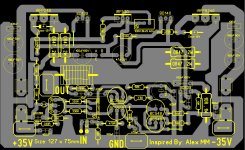
PCB Second Attempt...
Alex told me that is using Sprint Layout 5.0 so I decide to give myself a try. After a day for trying to learn the software and another for creating some custom elements and yet another day for drawing I came up with a new PCB.This software is difficult but it have much more capabilities than ExpressPCB so it worth it to start learn it.
So here it is. It is not perfect but don't forget that I'm still learning Any comments are welcome!
Regards!
Alex told me that is using Sprint Layout 5.0 so I decide to give myself a try. After a day for trying to learn the software and another for creating some custom elements and yet another day for drawing I came up with a new PCB.This software is difficult but it have much more capabilities than ExpressPCB so it worth it to start learn it.
So here it is. It is not perfect but don't forget that I'm still learning
Any comments are welcome!Regards!
Attachments
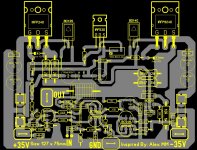
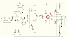
Hello People I'm back...again...
I want to present you my new update to the schematic.
I discovered that lowering the current trough the driver stage resulted in better sonic performance of the amplifier. I tried lowering it from near 50mA to near 25mA and results are excellent. I think that 50mA was too much...
The only thing that need to be changed is the resistor pointed on the picture from 220R to 330R.
Now enjoying the even better sound
Wish you all the best.
Attachments
I discovered that lowering the current trough the driver stage resulted in better sonic performance of the amplifier.
The only thing that need to be changed is the resistor pointed on the picture from 220R to 330R.
Are you lowering the driver current or increasing the output current?
The IRF loves much current for sure.Are you lowering the driver current or increasing the output current?
Lowering the driver current and yes they love much drive and idle current but that's the result that I experienced - it is a bit paradoxical isn't it.
Simulation also confirms my discovery it shows less THD but this can't be absolute accurate - we know very well that sim's and real world are two completely different things.
Regards!
Simulation also confirms my discovery it shows less THD but this can't be absolute accurate - we know very well that sim's and real world are two completely different things.
I think I'm lucky that I found simulation is very "accurate". The THD number is not accurate, but the relative performance most probably is. The difficulty is when each amp/setting has strength and weakness in different area, then it will be hard to judge which factor will decide the final performance.
- Status
- This old topic is closed. If you want to reopen this topic, contact a moderator using the "Report Post" button.
- Home
- Amplifiers
- Solid State
- What you think about this schematic?