So I've built up one of these, and have another two to go. I really like this project. The final product is a dense (like me!) board with lots of adjustability.
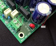
The board markings are a treat. Positive/negative legs marked for nearly everything. Even some + markings on the back side. Excellent. I like the vertical resistors. What a treat. No more measuring for spacing. Also the orientation of resistors (marked with a circle) diodes (marked with a circle and the anode identified) . Much appreciation here. I've held my breath soldering a few items that connect to one of those large ground planes and just hope for the best when the solder doesn't flow to the other side of the board, but otherwise have had little trouble with the work.
I took the time to set up my shopping cart on Mouser with the associated part ID from the original spreadsheet. This helps speed me along the build because the parts are already identified on the boards. Maybe everyone else does this, but I just realized how handy it is.
Thanks, Mark, for a great project to work on! Can't wait to fire it up!")
The board markings are a treat. Positive/negative legs marked for nearly everything. Even some + markings on the back side. Excellent. I like the vertical resistors. What a treat. No more measuring for spacing. Also the orientation of resistors (marked with a circle) diodes (marked with a circle and the anode identified) . Much appreciation here. I've held my breath soldering a few items that connect to one of those large ground planes and just hope for the best when the solder doesn't flow to the other side of the board, but otherwise have had little trouble with the work.
I took the time to set up my shopping cart on Mouser with the associated part ID from the original spreadsheet. This helps speed me along the build because the parts are already identified on the boards. Maybe everyone else does this, but I just realized how handy it is.
Thanks, Mark, for a great project to work on! Can't wait to fire it up!
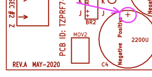
I mark the positive terminals of electrolytic capacitors with a "+" sign on the bottom silkscreen layer, just to give builders a way to double-check the polarity AFTER the board has been stuffed and soldered.
If the components are densely packed on the PCB, markings on the top side can become difficult or impossible to read. But you can still read the polarity band on the cap itself, then flip the board upside down and verify that it matches the polarity marked on the bottom side. Granted, this can be a little clumsy-- but it's a whole lot better than no possibility of double-checking at all. You get a little extra reassurance that you didn't stuff the capacitor backwards, and it doesn't impact board size or cost. Cost = zero, Benefit > zero, easy decision.
_
Attachments
Boy, it’s tough to get solder to flow correctly into a ground plain pad. The non-plane ones can be easily soldered at 620F/325C. I’ve been up to 700F/370C and even with flux the pad doesn’t get covered easily, especially on the large electrolytics!It's a four layer board and two of those layers are ground planes. You're heating up a LOT of copper when you solder a VRDN board. Increase tip temperature, patiently wait for solder to melt and flow. It will probably require more heating time than you're accustomed to. Pause every twenty solder joints and inspect with high power magnifier.
I have a Metcal PS-900. For most work I swear by it: it works great. But with it's "smart heat" temperature control (meaning I let the system choose the tip temperature) I never actually know how hot it is. Metcal talks of "power output" and "Frequency" but not actual tip temperature! For a VRDN board, this does cause some worry while I build. As mentioned, I'm trying to believe that the heat while soldering is going to the ground plane (it probably is) but with parts like transistors I still wonder!
If the solder doesn't melt then you can be pretty sure the temperature of the joint-being-soldered is below the solder melting temperature.
I set my Hakko to 405 degrees C and solder VRDN boards using a 3mm (1/8 inch) chisel tip plus eutectic 63-37 solder from Multicore. Works just fine for me.
I set my Hakko to 405 degrees C and solder VRDN boards using a 3mm (1/8 inch) chisel tip plus eutectic 63-37 solder from Multicore. Works just fine for me.
I did a silly thing and attached D3 with the wrong polarity. (As a result, I could not adjust the voltage on the positive side.) Worse, in my effort to extract the diode without unsoldering a bunch of other stuff, I seem to have destroyed the pads. So I am looking for a way to solder a diode into an appropriate place.
Looking at the schematic and testing a blank board, it appears I could solder it between the square pads of R7 and R11, with the cathode (banded end) going to R11 and the anode on R7. And, lucky me, those are already the ends I have sticking up, with exposed wire.
Before I do this, can someone confirm that this is correct?
I recommend you carefully and intensively study post #134 of the Scourge, Bulwark discussion thread (here is a link). Flying wirelead recommendations from the designer, are present on BOTH the schematics AND the PCB silkscreen. Your job as a builder is to follow the recommendations on the PCB. If you do, then the flywire indicators on the schematic will be trustworthy and accurate. If you ignore them --- well, as the minister says to Sheriff Bart in the final minutes of Blazing Saddles --- Son, yer on yer own.
I seem to have destroyed the pads
I recently installed D3 and D4 into the D5 and D6 locations. Yeah, oops... I was lucky enough to be able to remove the parts and excess solder (and not the pads) but it cost me a bundle in that I ended up purchasing a desolder station to do the work. Hmm. Yes, the 4-layer 3 ground plane boards can be challenging!
Your new solder location looks correct - so says the schematic. Just double check the orientation before soldering it down. (I know you will this time!)
BTW: Geez, Mark. That flying wireloop reference is something I never knew before. Cool!
If one wished to go off-piste and use a VRDN at say +/- 24Vdc.
Would a good way to do it be to change R7/R10 to 2.5k for a total series resistance of the R7/R8/VR1 and R9/R10/VR2 complexes of 4.18K and thus allow up to: 24.66Vdc.
Assuming of course that capacitors were uprated etc.
Other than this being unverified, is there anything that makes this a fundamentally dumb idea?
Excellent questions.Can the MOV handle the extra voltage? What about the regulators, diodes and rectifier bridge? It's going to be more than just the resistors and caps. Or maybe those components are already in your "etc" list...!
Quick mental maths suggests I would want at least 29v before the regulator for the (as I understand) 5v dropout for the regulators.
2x 1.5v for the bridges (I think that is correct for a dual bridge arrangement).
Drop across the R3/R5 and R4/R6 would be 0.04v for the circa 50mA current I would be running.
That gives something like 32Vdc rails.
Working backwards I would need something like 23Vac secondaries on the transformer.
The bridges are 600v rated so I don't see a problem there.
I can't find the specification in the data sheet but these regulators seem to be typically able to handle 35Vdc input.
1N4004 are 400v rated
1N4148 are 100v rated
The V05E40P has a rating of 40Vac and 56Vdc.
Those all look good to me.
I guess that answers the question. It should all work unless there is something else I am misunderstanding?
You've certainly done your homework, and the parts do appear that they might work. I'd think the original designer will say that this was not the intention of the circuit, however, but will probably also say hey, there are no guarantees by going off-piste with the design. If you can get it running and stable then hats off to you!
Am I correct that an LM317/337 chip passing say 20mA doesn't need a heatsink?
By my calculations:
P = EI = 5v drop across the regulator x 0.02A = 0.1W
According to the data sheets for the recommended On Semi Reg The Thermal resistance from Junction to Ambient is 65C/W
Therefore 0.1W with no heatsink would be 0.1w x 65C/W = 6.5C Rise above ambient?
Have I missed anything?
By my calculations:
P = EI = 5v drop across the regulator x 0.02A = 0.1W
According to the data sheets for the recommended On Semi Reg The Thermal resistance from Junction to Ambient is 65C/W
Therefore 0.1W with no heatsink would be 0.1w x 65C/W = 6.5C Rise above ambient?
Have I missed anything?
- Home
- Amplifiers
- Power Supplies
- VRDN: bipolar regulator PCB for line level ckts: ±11V to ±20V @ 1.5A with "De-Noiser"