")
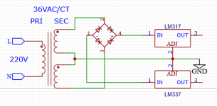
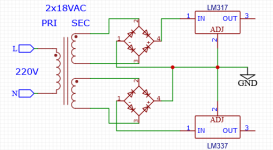
The VRDN design in post #1 of this thread is a four layer PCB.
It's easy to imagine that a talented PCB artist with lots of practical experience, could lay out the very same circuit topology on a 1-layer PCB or a 2-layer PCB, and get results that are almost as good as this 4-layer board. The reduced layer count would probably reduce PCB manufacturing cost and shorten the PCB fab delay / throughput time -- but the board size might be different.
It's easy to imagine that a talented PCB artist with lots of practical experience, could lay out the very same circuit topology on a 1-layer PCB or a 2-layer PCB, and get results that are almost as good as this 4-layer board. The reduced layer count would probably reduce PCB manufacturing cost and shorten the PCB fab delay / throughput time -- but the board size might be different.
I am currently working on a 1-layer traces + 1x ground plane version of that exact schematic, including the jumpers for half rectification (total= 2x layers; top & bottom). It shares the same BOM, some corrections to the silk screen regarding materials, and compatibility to nice aluminium cheap chinese heatsinks ♥️
Just inform me if you are interested
Just inform me if you are interested
Mark is it ok to post here or do you want me to start a new thread?The VRDN design in post #1 of this thread is a four layer PCB.
It's easy to imagine that a talented PCB artist with lots of practical experience, could lay out the very same circuit topology on a 1-layer PCB or a 2-layer PCB, and get results that are almost as good as this 4-layer board. The reduced layer count would probably reduce PCB manufacturing cost and shorten the PCB fab delay / throughput time -- but the board size might be different.
Please feel free to start a new thread to discuss your new circuit board, and remember to give your new board a new name without the character string "VRDN". That way there's no confusion and builders of your board / readers of your thread, will have a way to find it quickly, easily, and unambiguously.
If your max output current is some other number besides 1.5 amperes (due to different heatsinks and/or different amounts of filter capacitance), you may want to mention Iout_max in the title too.
Best wishes! MJ
If your max output current is some other number besides 1.5 amperes (due to different heatsinks and/or different amounts of filter capacitance), you may want to mention Iout_max in the title too.
Best wishes! MJ
Last edited:
Thanks Mark, in reality though it is not just based on your design, schematic-wise it is your design, how could I possibly omit the VRDN name and give it another name?Please feel free to start a new thread to discuss your new circuit board, and remember to give your new board a new name without the character string "VRDN". That way there's no confusion and builders of your board / readers of your thread, will have a way to find it quickly, easily, and unambiguously.
If your max output current is some other number besides 1.5 amperes (due to different heatsinks and/or different amounts of filter capacitance), you may want to mention Iout_max in the title too.
Best wishes! MJ
There are practical problems. I would have to copy your entire first post for the thread to make sense. It would be getting way too complicated for just a redraw of your schematic, called “the VRDN”.
What do you propose?
Also consider that the same BOM applies to my design, components have the same name and if something doesn’t work correctly on one board, it will very likely not work on the other board as well.
So what is the point?
I could name it “a copy of the VRDN”?
Last edited:
What's the point? The point is: the technical support person for the reduced layer count board is you. "I built the 2 layer board and it doesn't work, help me please!" goes in your thread and you shepherd the replies.
If you adamantly insist upon including the original acronym you could call your board "Reducto_VRDN" or "Cheapo_VRDN" or "Slimmer_VRDN" or, best of all, "SeeYou_VRDN"
If you adamantly insist upon including the original acronym you could call your board "Reducto_VRDN" or "Cheapo_VRDN" or "Slimmer_VRDN" or, best of all, "SeeYou_VRDN"
Here you go: my 2x layer version for those willing to etch some copper!
https://www.diyaudio.com/community/...t-pcb-layout-from-the-known-schematic.406415/
Thank you Mark Johnson!
https://www.diyaudio.com/community/...t-pcb-layout-from-the-known-schematic.406415/
Thank you Mark Johnson!
Page has been updated, please take a look:
https://www.diyaudio.com/community/...t-pcb-layout-from-the-known-schematic.406415/
thanks
https://www.diyaudio.com/community/...t-pcb-layout-from-the-known-schematic.406415/
thanks
As soon as you've built it and verified it works properly, I'll edit VRDN post #1 and add a link to your new thread.
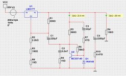
@Elvee has shown how it is possible to tweak D-Noizator further.
In this POST
I have done some test on that concept. Using submitted schematic.
By changing 2 resistors, 560ohm and 56kOhm.
The tradeoff is increased current from 6mA to 20mA.
On this graph
Red = De-Noiser disabled
White = VRDN Original
Yellow = VRDN Tweaked for ~6dB improvment

In this POST
I have done some test on that concept. Using submitted schematic.
By changing 2 resistors, 560ohm and 56kOhm.
The tradeoff is increased current from 6mA to 20mA.
On this graph
Red = De-Noiser disabled
White = VRDN Original
Yellow = VRDN Tweaked for ~6dB improvment
Attachments
- Home
- Amplifiers
- Power Supplies
- VRDN: bipolar regulator PCB for line level ckts: ±11V to ±20V @ 1.5A with "De-Noiser"