So I've built up one of these, and have another two to go. I really like this project. The final product is a dense (like me!) board with lots of adjustability.
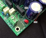
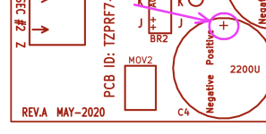
The board markings are a treat. Positive/negative legs marked for nearly everything. Even some + markings on the back side. Excellent. I like the vertical resistors. What a treat. No more measuring for spacing. Also the orientation of resistors (marked with a circle) diodes (marked with a circle and the anode identified) . Much appreciation here. I've held my breath soldering a few items that connect to one of those large ground planes and just hope for the best when the solder doesn't flow to the other side of the board, but otherwise have had little trouble with the work.
I took the time to set up my shopping cart on Mouser with the associated part ID from the original spreadsheet. This helps speed me along the build because the parts are already identified on the boards. Maybe everyone else does this, but I just realized how handy it is.
Thanks, Mark, for a great project to work on! Can't wait to fire it up!")
The board markings are a treat. Positive/negative legs marked for nearly everything. Even some + markings on the back side. Excellent. I like the vertical resistors. What a treat. No more measuring for spacing. Also the orientation of resistors (marked with a circle) diodes (marked with a circle and the anode identified) . Much appreciation here. I've held my breath soldering a few items that connect to one of those large ground planes and just hope for the best when the solder doesn't flow to the other side of the board, but otherwise have had little trouble with the work.
I took the time to set up my shopping cart on Mouser with the associated part ID from the original spreadsheet. This helps speed me along the build because the parts are already identified on the boards. Maybe everyone else does this, but I just realized how handy it is.
Thanks, Mark, for a great project to work on! Can't wait to fire it up!
I mark the positive terminals of electrolytic capacitors with a "+" sign on the bottom silkscreen layer, just to give builders a way to double-check the polarity AFTER the board has been stuffed and soldered.
If the components are densely packed on the PCB, markings on the top side can become difficult or impossible to read. But you can still read the polarity band on the cap itself, then flip the board upside down and verify that it matches the polarity marked on the bottom side. Granted, this can be a little clumsy-- but it's a whole lot better than no possibility of double-checking at all. You get a little extra reassurance that you didn't stuff the capacitor backwards, and it doesn't impact board size or cost. Cost = zero, Benefit > zero, easy decision.
_
Attachments
Boy, it’s tough to get solder to flow correctly into a ground plain pad. The non-plane ones can be easily soldered at 620F/325C. I’ve been up to 700F/370C and even with flux the pad doesn’t get covered easily, especially on the large electrolytics!It's a four layer board and two of those layers are ground planes. You're heating up a LOT of copper when you solder a VRDN board. Increase tip temperature, patiently wait for solder to melt and flow. It will probably require more heating time than you're accustomed to. Pause every twenty solder joints and inspect with high power magnifier.
- Home
- Amplifiers
- Power Supplies
- VRDN: bipolar regulator PCB for line level ckts: ±11V to ±20V @ 1.5A with "De-Noiser"