I agree with Nikwal's drawing, solves too many problems to ignore.
The IRF240 takes more current swing to drive at 22KHz than the
previously specified BJT, but there is no base diode to pump. IRF
610 might be more appropriate in this part of the circuit (far less
Miller), but the old 240 can squeak by.
More identical parts = cheaper...
I tried 9240 MOSFET in the Triodlington too, but gate drive was
sucking too much Miller to keep the Triode's plate at a constant
current. BJT wins this one. But a 9610 here might have been a
different contest. Good enough is still good enough, and I don't
want too ask unusual parts on the final Bill of Materials.
I only assume APEX stocks parts I see in his existing schematics?
I've not yet seen him to post any MOSFET but (9)240.
Attachments
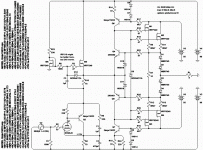
I dont have experience with tube circuits,... in my opinion IRF240 / 9240 is working but are not good choice for linear amplifier because not really complementary, this devices are to different
I prefer in my solid state designs quasicomplementary Mosfet output stage with excellent results
I prefer in my solid state designs quasicomplementary Mosfet output stage with excellent results
I dont have experience with tube circuits,... in my opinion IRF240 / 9240 is working but are not good choice for linear amplifier because not really complementary, this devices are to different
I prefer in my solid state designs quasicomplementary Mosfet output stage with excellent results
I have built both complimentary 240/9240 and quasi 240 and preferred the sound of the quasi.
I dont have experience with tube circuits,... in my opinion IRF240 / 9240 is working but are not good choice for linear amplifier because not really complementary, this devices are to different
I prefer in my solid state designs quasicomplementary Mosfet output stage with excellent results
I totally agree (9)240 are terrible compliments (without crossing correction).
Thats why this output stage quasicompliments on Schottky diodes instead.
Where there is not allowed any loop NFB, we can't rely upon that to fix the
crossing for us. It has to be corrected locally, in a most direct coupled way.
Maybe this correction is a loop too? But a very short one.
Ok, I do allow myself one slightly phase shifted loop feedback to the Cathode.
But its mostly Positive, and purposed to remove a NFB that otherwise fights
against the Triode's rule of Mu. I don't think it breaks the spirit of the quest.
Its a very old and traditional tube hack (Loftin White) anyway.
Last edited:
I totally agree (9)240 are terrible compliments (without crossing correction).
Thats why this output stage quasicompliments on Schottky diodes instead.
Where there is not allowed any loop NFB, we can't rely upon that to fix the
crossing for us. It has to be corrected locally, in the most direct coupled way.
The (9)240 are basically switching MOSFETs according to the spec.
However, I think you can make a decent sounding amp with them.
I have made around 40 complimentary amps using (9)240's and had no complaints from customers.
Just finished a quasi 240 design and it does sound a little brighter than the complementary version. But that could be down to the extra driver required for the quasi.
D1+D2 are quasicompliments to D3+D4. Mosfets only
trusted here to do the hot work, not make decisions.
I can show you one where I change one half entirely
to BJT, and it still crosses exactly the same. If you
need proof the diodes are the quasicompliments. And
MOSFETs "compliments" are topological convenience
not in any way related to the final crossing behavior.
Last edited:
We are maybe not comparing apples to apples?
1) crossing mosfet (square law cutoff) against loosely matched complimentary cutoff. Hot mosfets rule.
2) crossing emitter (log law cutoff) with complimentary, reasonably matched cutoff. Mosfets are slave.
3) crossing Schottky (square law cutoff) with exact matching quasicompliment. Mosfets are slave.
A) Amplifier with no feedback, and an uncorrected crossing distortion.
B) Amplifier with loop NFB to correct both crossing and other distortions.
C) Amplifier with local direct coupled feedback to correct crossing distortion only.
Since this is 3) and C), I think we are dealing with a whole new animal.
Unlikely to sound like IRF(9)240 circuits of past experience.
Last edited:
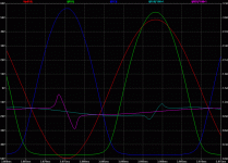
Let the picture do the talking regarding who, what, crosses how???
Note: The gate drive currents are not shown to scale, but I*100+1A
Mismatch of the MOSFETs is having much more effect at the peaks
than through the crossing... Though some of it is 2nd Harmonic due
to the tube up front.
Note: The gate drive currents are not shown to scale, but I*100+1A
Mismatch of the MOSFETs is having much more effect at the peaks
than through the crossing... Though some of it is 2nd Harmonic due
to the tube up front.
Attachments
Last edited:
have found this
MATCHING P-CHANNEL AND N-CHANNEL MOSFETS
It is impossible to produce a P-channel power MOSFET that has the same electrical characteristics as an N-channel power MOSFET. Because the mobility of carriers in an N-channel power MOSFET is about 2.5 times to 3 times higher, for the same RDS(ON) value, the P-channel power MOSFET size must be about 2.5 times to 3 times that of an N-channel power MOSFET. Because of the larger area, the P-channel device will have lower thermal resistance and higher current rating. Its dynamic performance (capacitance, gate charge, etc.) would be affected proportionally by the chip area.
In low-frequency switching applications in which conduction loss is dominant, the P-channel MOSFET should have a current rating similar to that of the N-channel MOSFET. If two MOSFETs have the same current rating, then their junction temperatures can be thought to be similar at the same case temperature and the same current. In this case, the P-channel MOSFET chip area is 1.5 ~ 1.8 times that of the N-channel MOSFET chip area.
In high-frequency switching applications in which switching loss is dominant, the P-channel MOSFET should have similar total gate charge to that of the N-channel MOSFET. If two MOSFET have the same gate charge and are driven in a similar way, then their switching losses are similar. In this case, the P-channel MOSFET has similar chip area and the current rating is lower than that of N-channel MOSFET.
For operation in linear mode, we need to match P-channel and N-channel devices with similar FBSOA characteristics in the real operating area. Frequently, this means the same rated Pd, but attention needs to be paid to the ability of the device to operate in this mode.8 In real applications, the suitable P-channel must be carefully selected in between the same current rating and the same gate charge. Applications requiring the same RDS(ON) are very rare.
MOSFETs in a Class AB amplifier require extended FBSOA characteristic as they operate in linear mode. Power dissipation would be high because of linear operation.
The quasi configuration is a virtual device anyway.
The MOSFET does not operate upon its own curve.
It is corrected to operate upon a different curve.
You see the 22KHz +/-50V graph above? The gates
are purposely not driven linearly, nor identically, only
an identical complimentary square law result matters.
Since when crossed, this becomes a linear function.
Carve a pair of identical statues out of larger rocks.
Obviously both rocks do not have to start identical,
only both larger FBSOA then the desired final result.
And yes, drive has fewer hoops to jump through if
Qg/Gm of both big rocks is similar. But exact match
not essential.
Last edited:
Well, things ain't goin' so swell.
One step forward, three steps back.
I got models for all APEX's parts now,
and all seem to be working fine.
On the other hand... I've tried twenty
ways from Sunday to plug back in the
current limiting feature... Either goes
wacky at clipping or crossing or both.
I'm not sure why I can only seem to
swing +/-50V, when I got plenty of
gate drive voltage and current? At
that magic threshold it goes nutz...
If I keep playing with it, something
will eventually work.
From Thread: 100W Ultimate Fidelity Amplifier
I can't seem to get drive shunting current limiter to work in concert
with crossing correction. Too similar, they stomp on each other? How
would you feel about your other protection circuit from 100W Ultimate
Fidelity grafted over to this design instead?
Ohyeah: LTSpice now has default models for BC337, and I tried those
as the comparator, and 2n5501 also. But klunky old MJE 340/350 sims
tons more stable than any comp I could throw around the higher gain
transistors. The sim really seems to like em, I don't understand why?
They were in your drawing, I assume you have plenty.
Here's where I am at so far... I'm not suggesting this is even close to
finished yet! Got a feeling that 600:600 transformer is not what you
had in mind, though it does offer a balanced option and ground loop
breaking. My samples here spec for no more than 4500Hz. Yet when
driven by lower than 600, into higher than 600, bandwidth expands
easily more than 20-20K. Maybe not every cheap transformer can do?
But these old Stromberg Carlson I got for a buck apiece certainly do.
You like it? You hate it (the transformer)? I can rig up something else...
I'll entertain any suggestions relevant to why the sim freaks out over
+/-50V output? Also how I can soft current limit without freaking the
sim or spoiling the ideal shape of the crossing? Just moving the points
of comparison outboard the source resistors one example that gives
the desired limiting, but also unacceptably distorts the crossing...
I think perhaps the Mu follwer stage has unlimited pull up current may
be part of the problem for simple limiting in the output stage. Seems
I've created a real complicated mess here...
Q1 + Q3 throwback to Dodson Hyperbolic. Seems R7 doesn't work to
maintain constant bleed when one gets too near the rail? Yet wastes
less power than rail CCS? So I've kinda thrown both type CCS for the
moment. Like I said: its in a total state of uncertain mess right now...
As long as you stay under +/-50V, and don't care about current limit,
the linearity is actually pretty darn good. But you can't have all these
other problems I've created for a box you might build to sell... I have
not lost sight the original purpose.
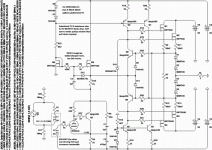
PRO pin must be connect to over-curent detector on amplifier circuit. Protect will be activeted with positive DC voltage (mosfet amp hv23), or ac voltage (PA amp B500). Unfortunaly this Hi-Fi amp have not over-curent detector circuit, and it must be add if you want use this pa protect with short-circuit protect. PA protect can work witout short-circuit protect, just not use PRO pin. Protect which I suggest early in this thread have short-circuit protect without over-curent detector on amplifier circuit. If you have no expirience to add over-curent detector circuit on this amp, is better to use this circuit.
Regards
I can't seem to get drive shunting current limiter to work in concert
with crossing correction. Too similar, they stomp on each other? How
would you feel about your other protection circuit from 100W Ultimate
Fidelity grafted over to this design instead?
Ohyeah: LTSpice now has default models for BC337, and I tried those
as the comparator, and 2n5501 also. But klunky old MJE 340/350 sims
tons more stable than any comp I could throw around the higher gain
transistors. The sim really seems to like em, I don't understand why?
They were in your drawing, I assume you have plenty.
Here's where I am at so far... I'm not suggesting this is even close to
finished yet! Got a feeling that 600:600 transformer is not what you
had in mind, though it does offer a balanced option and ground loop
breaking. My samples here spec for no more than 4500Hz. Yet when
driven by lower than 600, into higher than 600, bandwidth expands
easily more than 20-20K. Maybe not every cheap transformer can do?
But these old Stromberg Carlson I got for a buck apiece certainly do.
You like it? You hate it (the transformer)? I can rig up something else...
I'll entertain any suggestions relevant to why the sim freaks out over
+/-50V output? Also how I can soft current limit without freaking the
sim or spoiling the ideal shape of the crossing? Just moving the points
of comparison outboard the source resistors one example that gives
the desired limiting, but also unacceptably distorts the crossing...
I think perhaps the Mu follwer stage has unlimited pull up current may
be part of the problem for simple limiting in the output stage. Seems
I've created a real complicated mess here...
Q1 + Q3 throwback to Dodson Hyperbolic. Seems R7 doesn't work to
maintain constant bleed when one gets too near the rail? Yet wastes
less power than rail CCS? So I've kinda thrown both type CCS for the
moment. Like I said: its in a total state of uncertain mess right now...
As long as you stay under +/-50V, and don't care about current limit,
the linearity is actually pretty darn good. But you can't have all these
other problems I've created for a box you might build to sell... I have
not lost sight the original purpose.
Attachments
Last edited:
Now if I were completely primitive, I might want to know if tungsten
lamps could replace those 0R47? The Sylvania 211-12 supposedly
is 0R85 ohms cold? So at least two in parallel. For each source...
I need more info how lamp resistance ramps vs power dissipation.
I'm not serious here, just daydreaming...
As for why 20mA??? Did you ask the diode bias current 20mA, or the
constant current source and sink at the collectors 20mA?
Its cause the input can swing +/-20mA into the node between the
emitters. Gate pull-up and pull-down CCS must sink similar amounts
of current to fully utilize that drive capability. Actually there is an
unresolved problem that the Mu follower can pull unlimited current.
And any attempt to resist above the drain creates a voltage swing
that aggrivates the Mu Follower's Miller.
If you meant 20mA on the diode? Thats just so MOSFET reference
diode drop closely cancels the offset of the 20mA Mu Follower.
There still has to be some downward pull, even with the tube cold,
else nothing about the Mu Follower prevents the voltage to rise...
Not saying any of this is a good idea, or will stay. You just asked
what the heck was I thinking??? I've done my best to explain...
Last edited:
And my earlier question why I can't out beyond +/-50V?
I've added it up. The missing 5V is all lost in RDS, source
resistors, and Schottky stack. Its not a drive issue, it
just ran outa steam earlier than I had guestimated...
Even +/-50V sine amounts to 150WRMS into 8 ohms...
OR47 might be a bit excessive in series with Diode that
will actually do the real current shaping. 0R22 seems a
more plausible number?
I still want current limit to knee in gently at around 6A.
So many ways to do that.. But which is best? Most of
the simple solutions have failed to impress in LTSpice.
Last edited:
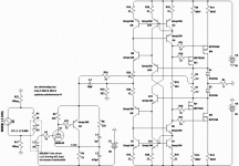
Sorry temporary inside-out current-mirror sillyness.
Just more of my aborted struggles with the current
limiters. Not actually relevant to the latest news.
What development was important to post: Has more
to do with the need for mu Follower to have an equal
pull up and down slew capability. Then it hit me!
Why not abuse entire output stage as a Mu follower?
No slew imbalance to fight against soft current limits
that will soon go back in circuit. Less parts, a whole
+90V rail that was there before, not needed anymore.
OK, maybe not less parts right at the moment, with
those crazy 3way current mirrors... Unlikely to stay.
Attachments
Last edited:
You have so many creative ideas.Sorry temporary inside-out current-mirror sillyness.
Just more of my aborted struggles with the current
limiters. Not actually relevant to the latest news.
What development was important to post: Has more
to do with the need for mu Follower to have an equal
pull up and down slew capability. Then it hit me!
Why not abuse entire output stage as a Mu follower?
No slew imbalance to fight against soft current limits
that will soon go back in circuit. Less parts, a whole
+90V rail that was there before, not needed anymore.
OK, maybe not less parts right at the moment, with
those crazy 3way current mirrors... Unlikely to stay.
Regards
Creative??? I guess thats one polite way to describe it...
I steal a load of ideas then implement them incorrectly?
---
My earlier problem with limiters:
Any attempt to shunt an offending
gate toward cutoff (toward center),
had nasty side-effect to also shunt
the opposing gate into a complete
hard cutoff (much closer to cutoff
to begin with). And pull the drive
signal itself toward the offending
rail!
The correction circuit can only
pull inward, so had no power to
enforce common sense over this
inward pulling madness! Worse,
just fooled correction circuit
transistors to shut down too...
So thats why I have it all turned
inside out for the moment... Shunt
either gate toward cutoff (toward
rail), has side effect to turn ON
the opposing MOSFET. An inward
pull correction circuit can sucessfully
fight against this orientation of
unwanted error (through the mirror).
Also preventing unwanted shutdown
of the correction circuit. And pull
drive away from the rail too. (half
baked theory)
Is there is a better way to do all
this turned rightside-out? I havn't
figured anything that works yet...
---
Loftin White circuit is out of tune
now... You can graph +/-15mA in the
470uF bypass cap! I suspect the Mu
Follwer Gyro's self-centering resistor
R10 is too small value for plate load?
I measure big AC current leak here.
Inductor I had goten rid of earlier
might want to come back...
Or maybe I'll take another crack at
a real servo??? I suspect it didn't
work before for same reason as the
limiters. Maybe no problem anymore?
Last edited:
- Status
- This old topic is closed. If you want to reopen this topic, contact a moderator using the "Report Post" button.
- Home
- Amplifiers
- Solid State
- Tube/Mosfet 100W Hybrid Amplifier