Agus Widarto said:Hai all of DIY'er can you tell me to make good PCB with the simple process? last time i am make Aleph PCB the are bad!
Mr Fotios please helps me ????

Thank and God Bless You all!
Hi Agus
Here i am! Maybe some other members gave you the method for making PCBs at home but I don’t have the time to read their posts. My own way to making my custom PCBs (single or double sided) it is the next:
1.. I use only presensetized pcbs concretely those with the blue shelf adhesive cover because are not so delicate in light exposure and I know that they need from 10 to 12 minutes of exposing in UV light (some times and 15 minutes are not dangerous).
2..During the designing of pcb, if it has thin lines always I fill the unused area with copper pour (most of pcb drawing programs make this automatically) so the etching process it is as faster as possible and the pcb not remains for long time in the etching acid solution.
3..To print the films I use only an inkjet printer of Epson with original black ink and original transparencies also of Epson. For a better opacity of the routes and copper areas I make this trick. In the setup menu before the printing, I don’t declare the transparency film as transparency, but as photo quality inkjet paper because the printer under this selection it jets the most possible quantity of ink and the Epson transparencies are incredible sucking. They dry after 2 minutes! Many people use laser printers with laser transparencies or transparent paper. The disadvantage of the laser printing it is the shrinking of paper and the loss of 2 to 3 mm of the original drawing dimensions because the printing is thermally processed. Instead the inkjet printing it is cold and there is no danger of lost in dimensions. Believe me I tried in the past this method of laser printing and I had rejected him from the beginning. The films printed always as positive with the component side mirrored so the printed side of transparency will be in absolute contact with the copper (to avoid any gap or else the thin lines will be thicker)
4..After the preparing of the film, I cut a little larger piece of copper clad board from the film. Now I go to the dark room. With only the dark lamps (red color) lighted, I remove the shelf adhesive from the board and I place on it the film with its right side faced to me and I stick it with two or three pieces of transparent tape on the board. I place the board between two glasses and I press the resulted sandwich with 4 paper clips.
5..Now it is the time for the exposure in UV light. You can use simple fluorescent lamps or for better a lamp of Hg steams. Place the sandwich under the lamp, and leave it for 10 to 12 minutes. Be careful that the light it is applied in a uniform manner onto the whole board.
6.. Now the development. The most chip development liquid it is a solution of NaOH (the common caustic soda for pipe obstuction) in water. Two teaspoon in 1 lt water it is enough. Use only bottle of glass, warm the solution about 30⁰C and shake it well by loosen sometime the cap of bottle for exhausting the gasses produced. And don’t forget the protective gloves! Pour now enough solution into a plastic bowl, and turn on only the dark light lamps. Disassemble the sandwich, remove the film from the board and put it into the developer solution. Move the board slowly into the liquid and after few seconds the drawing will appears on the copper surface because the developer removes the photo resist which have been lighted from the UV. Continue until you are sure that all the drawing lines appeared. After this there is no need furthermore for dark rooms. Rinse well with water the PCB and you are ready for the etching process. Before this, inspect well the lines on the board and if they are any bad point correct it with a permanent marker.
7..For the etching I use a little danger way. I use a solution of thinned hydrochloric acid with water (I have buy a 25lt can of 98% clear HCL acid and I have thin it with water by 50-50) but you can use also the well known Aqua Forte (a solution of 15% HCL in 85% water of course most weak and the time of etching most long). To accelerate the etching process, I add a small amount of 98% clear Hydrogen Peroxide (known as Perydrol) which have the property to warm quickly the HCL solution and thus make it yet more effective by reducing the etching time in 5 minutes as much for a board of 200 X 300 mm for example. Be careful with the vapors! Also the Perydrol it is most caustic from the HCL!
8..After the finish of etching, we rinse the board well with water and we don’t remove the fixed photo resist from the tracks before drilling holes. After the drilling completion, we rinse the board with alcohol to remove the photo resist and we rub the copper with wire sponge or some similar. Finally we spray the board with a protective lacquer to avoid the corrosion of copper.
That is all. If I had the time I will post some photos. Maybe another day. For making double sided boards, it is a more difficult work and must be explained separately because the tricks used are so much. And this in another day.
Fotios
sandstorm33 said:
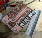
But then come the FUN!!!..Drilling the result. I have trouble keeping the small carbide drill bits from breaking .....Anybody got a system for successful drilling???
Your carbide drill bits broken because your drilling motor it plays a little in the press drill stand. I had the same problem with my Dremel drill and stand. With it you can use only HSS bits because are more flexible from those of carbide. I use now the new turbo shank carbide drill bits only in my router table vice (appropriate jaw of 3,154mm for the clamping in motor) with success because the vice it is absolute stable during the vertical sliding.
Fotios
Is it really worth the time an effort to make PCBs yourself?
You can get them made pretty cheaply, I use www.pcbcart.com
You can get them made pretty cheaply, I use www.pcbcart.com
Dave said:Is it really worth the time an effort to make PCBs yourself?
Yes. You can have it within hours, rather than dats (or weeks). It doesn't look as pretty, but works just as well and is cheaper once you have the hang of it.
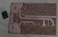
I did this one with Tom Gootee's method:
Attachments
Dave said:Is it really worth the time an effort to make PCBs yourself?
You can get them made pretty cheaply, I use www.pcbcart.com
Of course i think that we speak about prototype designes. Usually i make very complex and large pcbs and thus the mistakes are very common. In the past i ordered my prototypes in a local lab. The problem was that either for one or for ten pcbs the cost was the same. I have a big 32in TV packing box in my warehouse foul of useless boards. After this i decided to make my own mini pcb lab. Moreover the time that i spend to draw a pcb in PC it is by 1000 times more than to construct the pcb. If the prototype has success and the errors corrected then i order the pcbs from the lab. And something other. China it is far from my place. So, for a pcb of 10 Euro for example the shipping cost it is from 20 to 40 Euro! I had paid before 5 months for a cost free mini parcel (0,5Kgr!) of 200 special resistors from a factory in China, 90 Euros!!! in DHL for the tracking to north Greece where is my home. You are sorry for this, but i am very sorry because ME i paid the bill!
Regards and thanks for the matchmaking

Fotios
just curious.... do they even make "dry transfer" etch resist kits anymore????
i used to use dry transfer to place the pads for the components, then make the traces with etch resist tape, or an etch resist pen (a.k.a. a "sharpie" permanent marker). i also used machinists's setup ink to coat ground plane areas, as it made a very convenient etch resist that could be brushed on.
also FeCl is probably a lot safer to have around than H2SO4 or HCl...... used to have a cat that would lick up drips of FeCl when i was working on boards. i always shooed her away, but it never seemed to harm her....
Agus Widarto said:Hai all of DIY'er can you tell me to make good PCB with the simple process? last time i am make Aleph PCB the are bad!
Mr Fotios please helps me ????
Thank and God Bless You all!
Judging from the email I get, thousands of people are using the toner transfer method that I have described, here:
http://www.fullnet.com/~tomg/gooteepc.htm
If you can't get exactly the same type of paper, you might want to try some pages from a glossy magazine. It shouldn't matter if they have magazine ink on them (except for possibly impairing your ability to inspect them, or to align them for 2-sided boards). [I, myself, have not tried using magazine paper, but have gotten many emails from others who have successfully used it, with that procedure.]
Please note that I described the method in excruciating detail for a very good reason (AND to cut down on email questions about it
") . It should be done exactly as described, at least until you are getting perfect results and are experienced-enough to try your own modifications. (You would be amazed at how many emails I have gotten from first-timers who have blithely ignored, or completely changed, certain steps in the procedure, who then email me to ask why it wasn't perfect, or even once-in-a-while to actually complain!)
. It should be done exactly as described, at least until you are getting perfect results and are experienced-enough to try your own modifications. (You would be amazed at how many emails I have gotten from first-timers who have blithely ignored, or completely changed, certain steps in the procedure, who then email me to ask why it wasn't perfect, or even once-in-a-while to actually complain!)Regarding drilling:
I use solid carbide bits with 1/8-inch shanks. I buy the used 'repointed' ones, for about $20 for a box of 50 (last time was on ebay, I think). I use a Dremel-like rotary tool, clamped onto a cheap little drillpress (with a piece of scrap metal and some large U-bolts), from which I removed the original motor, etc. I usually only break bits when I hit them with my hand, or something.
I think that the key to making it work, without breaking the bits, was attaching two springs, between the drillpress's 'post' (the part that doesn't move) and the part that carries the rotary tool, so that it is held under tension, which removes most of the horizontal 'play', from the moving part of the drillpress mechanism.
I used to use the high-speed steel ('wire gauge') bits. But they get too dull way too quickly, for me; within 100 to 300 holes, even with a slower drill. I run my tool at 30,000 RPM and can sometimes drill several thousand holes with one .032-inch carbide bit, before I accidentally break it (usually by bumping against it with something, while the drill is off).
P.S. For the 'hardcore' PCB-makers among you, there is a ton of good stuff about it in the message archive of the Homebrew_PCBs discussion group, at http://www.yahoogroups.com . For toner transfer, there are descriptions of how to modify small laminating machines to automate the transfer process. There are even detailed descriptions of how to modify certain inkjet printers so you can print the PCB pattern *directly* onto copperclad pcboards!
Nowadays, for production runs, I usually just go to http://www.4pcb.com . If nothing else, at least try their on-line FreeDFM utility.
Dave said:Is it really worth the time an effort to make PCBs yourself?
Erm, have you looked at the title of this website recently?
Re: Re: To Make Good PCB at home
gootee said:
Judging from the email I get, thousands of people are using the toner transfer method that I have described, here:
http://www.fullnet.com/~tomg/gooteepc.htm
If you can't get exactly the same type of paper, you might want to try some pages from a glossy magazine. It shouldn't matter if they have magazine ink on them (except for possibly impairing your ability to inspect them, or to align them for 2-sided boards). [I, myself, have not tried using magazine paper, but have gotten many emails from others who have successfully used it, with that procedure.]
Please note that I described the method in excruciating detail for a very good reason (AND to cut down on email questions about it
------------------------------------------------------------------------------------
Thank you very .......very much gootee for your information about the laser transfer. Today i byied some glossy papers of different thicknes to try transfer NOT in a PCB but in an aluminum face some logos of 0,3mm thick letters. According to your suggestions for my big surprise the experiment was absolute succesfull!! Thanks! You gave me a precious help. I tried with different solvents to remove te letters (alcohol, white spirit etc) and the only that removed slightly the pattern letters was the nitric solvent! In all others the printing withstands verry well! In hot water the paper removed very easy in 5 minutes! And voila a nicefull label such a silcscreen. The transfered toner it is very stable! Now i try to scrape it with my nail but it is very strong! Your method it is nice! Thanks again. As for the copper of PCB i don't have any doubt that it works perfectly. Thanks because you save me from the tiring process and the expenses of my previous method of photoetchant.
Congratulations. You are a big craftsman!
Fotios
Re: Re: Re: To Make Good PCB at home
fotios said:gootee said:
Judging from the email I get, thousands of people are using the toner transfer method that I have described, here:
http://www.fullnet.com/~tomg/gooteepc.htm
If you can't get exactly the same type of paper, you might want to try some pages from a glossy magazine. It shouldn't matter if they have magazine ink on them (except for possibly impairing your ability to inspect them, or to align them for 2-sided boards). [I, myself, have not tried using magazine paper, but have gotten many emails from others who have successfully used it, with that procedure.]
Please note that I described the method in excruciating detail for a very good reason (AND to cut down on email questions about it
------------------------------------------------------------------------------------
Thank you very .......very much gootee for your information about the laser transfer. Today i byied some glossy papers of different thicknes to try transfer NOT in a PCB but in an aluminum face some logos of 0,3mm thick letters. According to your suggestions for my big surprise the experiment was absolute succesfull!! Thanks! You gave me a precious help. I tried with different solvents to remove te letters (alcohol, white spirit etc) and the only that removed slightly the pattern letters was the nitric solvent! In all others the printing withstands verry well! In hot water the paper removed very easy in 5 minutes! And voila a nicefull label such a silcscreen. The transfered toner it is very stable! Now i try to scrape it with my nail but it is very strong! Your method it is nice! Thanks again. As for the copper of PCB i don't have any doubt that it works perfectly. Thanks because you save me from the tiring process and the expenses of my previous method of photoetchant.
Congratulations. You are a big craftsman!
Fotios
Hi Fotios,
Well, thank you for your 'thank you'. You are welcome. It is gratifying to know that it has helped you.
Yeah, I forgot to mention that the process is also great for 'silkscreening' one-sided pcboards, and for putting artwork onto metal (and some plastics etc), e.g. for instrument panels.
I really-appreciate your very kind words. But my original contribution toward this type of process was not really as great as you make me sound. I first researched the existing efforts and then mainly just contributed a lot of trial-and-error experimentation. That did require a lot of time, and quite a bit of money for trying many different types of paper, etc. So, after I found a method that worked well for me, I decided that it would be a good thing if others would not have to 're-invent the wheel', as they say. So I decided that I should put the details onto a webpage.
Thanks again.
Re: Re: Re: Re: To Make Good PCB at home
Hi Tom
You are very modest, really! I am 49 years old and I am occupied with electronics from my 10s. This means from 1970 in my uncle lab who was repaired tube radios and TVs. I remembered the admiration of all for the first solid state radios (they called transistors and not portable radios at that time in Greece; what wonderful days in that time, unforgettable days). So, for 39 years I am an experimenter with all about electronics and electrics. I am graduate of the Greek public higher schools of electrician and electronic engineers (8 years of educational in these schools after the total 12 years of the first and secondary degree education, thus total 20 years in school while I worked simultaneously because my father was died from cancer in 1970 in his 39s when I was only 11 and he leaved to our family only a house and a little death pension. I write them so you can understand that our thoughts, our practical our skill and our views converge. So, many times only the reference of someone for something it is enough for me to I get the opportunity for a practical test. I don’t need the many explanations and instructions; because as you understand for so many years I have heard already something about all and I have enough experience about chemicals and procedures (I hope to not hear us the FBI because we are scientists and not terrorists!). Just today I tried your method and I found that the baked toner removed easy with nitric solvent (that which sell the paint stores) but I don’t know if it causes corrosion in the copper; instead for aluminum it is the most drastic cleaner without any danger for corrosion in it. BTW a drastic corrosive for cleaning aluminum surfaces from little scratches (which also remove totally the anodizing if we want) it is a solution of enough caustic soda (NaOH) with light warmed water.
As for the glossy papers, I got by chance from the local store of Cartridge World (it is international www.cartridgeworld.com) 4 different in weight glossy papers free for test (140GSM-185GSM-210GSM-270GSM) and I tried the 210GSM with success from first. Tomorrow I will try some transfers in PCBs so for etching copper (I use as you the same etchant solution of thinned HCL acid with little Hydrogen Peroxide) as for a silkscreen on the PCB. I will post the results. As for the paper removing from the sticking toner on copper it is most easy if we leave the PCB to soak in warm water for 20 minutes at least; so the last remaining layer of paper which is the most difficult to removed it is done easiest with little rub from our finger.
For double sided boards, after the printing we iron the one side transfer paper on the board and after removing the paper we drill some pad holes (6 to 8 are enough) near the corners and the middle of PCB with 0,7mm drill bit. On the other side paper we drill exactly the same pad holes corresponding to the first side drilled holes, before we iron the paper. From the sticking and cleaned side pattern, we pass thru the drilled holes some sewing pins as guides and we put the other paper with the aid of pins exactly in the right place. We stick the paper in the corners with tape so don’t can moved and we remove the pins. Now we are ready for the ironing process.
For the stuff:
1…Ready thinned HCL (15-20% HCL solved in water) sell all the super markets known in my country as Aqua Forte.
2…The Hydrogen Peroxide offered in drugstores as a solution of 10% in water for wound cleaning but it is not appropriate for the etchant solution. Unfortunately the clean Peroxide (98% content) it is very caustic and you must have an acquaintance pharmacist (druggist?) to you, so you can get a bottle of clean Peroxide.
And don’t forget the nice printings which we can make with the same way on the front and back panels in the aluminum cases of our amplifiers etc. We can give a termination in tiring letterset transferring and the varnish coating. And probably we can get out of the clutches from the “masters” of expensive silkscreen labs.
Fotios
gootee said:
Hi Fotios,
Well, thank you for your 'thank you'. You are welcome. It is gratifying to know that it has helped you.
Yeah, I forgot to mention that the process is also great for 'silkscreening' one-sided pcboards, and for putting artwork onto metal (and some plastics etc), e.g. for instrument panels.
I really-appreciate your very kind words. But my original contribution toward this type of process was not really as great as you make me sound. I first researched the existing efforts and then mainly just contributed a lot of trial-and-error experimentation. That did require a lot of time, and quite a bit of money for trying many different types of paper, etc. So, after I found a method that worked well for me, I decided that it would be a good thing if others would not have to 're-invent the wheel', as they say. So I decided that I should put the details onto a webpage.
Thanks again.
Hi Tom
You are very modest, really! I am 49 years old and I am occupied with electronics from my 10s. This means from 1970 in my uncle lab who was repaired tube radios and TVs. I remembered the admiration of all for the first solid state radios (they called transistors and not portable radios at that time in Greece; what wonderful days in that time, unforgettable days). So, for 39 years I am an experimenter with all about electronics and electrics. I am graduate of the Greek public higher schools of electrician and electronic engineers (8 years of educational in these schools after the total 12 years of the first and secondary degree education, thus total 20 years in school while I worked simultaneously because my father was died from cancer in 1970 in his 39s when I was only 11 and he leaved to our family only a house and a little death pension. I write them so you can understand that our thoughts, our practical our skill and our views converge. So, many times only the reference of someone for something it is enough for me to I get the opportunity for a practical test. I don’t need the many explanations and instructions; because as you understand for so many years I have heard already something about all and I have enough experience about chemicals and procedures (I hope to not hear us the FBI because we are scientists and not terrorists!). Just today I tried your method and I found that the baked toner removed easy with nitric solvent (that which sell the paint stores) but I don’t know if it causes corrosion in the copper; instead for aluminum it is the most drastic cleaner without any danger for corrosion in it. BTW a drastic corrosive for cleaning aluminum surfaces from little scratches (which also remove totally the anodizing if we want) it is a solution of enough caustic soda (NaOH) with light warmed water.
As for the glossy papers, I got by chance from the local store of Cartridge World (it is international www.cartridgeworld.com) 4 different in weight glossy papers free for test (140GSM-185GSM-210GSM-270GSM) and I tried the 210GSM with success from first. Tomorrow I will try some transfers in PCBs so for etching copper (I use as you the same etchant solution of thinned HCL acid with little Hydrogen Peroxide) as for a silkscreen on the PCB. I will post the results. As for the paper removing from the sticking toner on copper it is most easy if we leave the PCB to soak in warm water for 20 minutes at least; so the last remaining layer of paper which is the most difficult to removed it is done easiest with little rub from our finger.
For double sided boards, after the printing we iron the one side transfer paper on the board and after removing the paper we drill some pad holes (6 to 8 are enough) near the corners and the middle of PCB with 0,7mm drill bit. On the other side paper we drill exactly the same pad holes corresponding to the first side drilled holes, before we iron the paper. From the sticking and cleaned side pattern, we pass thru the drilled holes some sewing pins as guides and we put the other paper with the aid of pins exactly in the right place. We stick the paper in the corners with tape so don’t can moved and we remove the pins. Now we are ready for the ironing process.
For the stuff:
1…Ready thinned HCL (15-20% HCL solved in water) sell all the super markets known in my country as Aqua Forte.
2…The Hydrogen Peroxide offered in drugstores as a solution of 10% in water for wound cleaning but it is not appropriate for the etchant solution. Unfortunately the clean Peroxide (98% content) it is very caustic and you must have an acquaintance pharmacist (druggist?) to you, so you can get a bottle of clean Peroxide.
And don’t forget the nice printings which we can make with the same way on the front and back panels in the aluminum cases of our amplifiers etc. We can give a termination in tiring letterset transferring and the varnish coating. And probably we can get out of the clutches from the “masters” of expensive silkscreen labs.
Fotios
Eva said:I find that positive presensitized PCB and inkjet transparencies are the easiest method. However, the four steps of the process should be done with great care because once something has gone wrong in one step you will have serious trouble to get the following steps right. On the other hand, good transparencies give a better error margin for UV exposure time. Optimum UV exposure time gives a good error margin for NaOH concentration in developer solution. Optimum developing results in almost fool-proof etching...
Hi Eva
Because i use exactly the same methods as you for etching process, i revised by some way my view after the post nr.32 of gootee. Take a look in posts 32,34,35,36 are very informative.
Fotios
Hi Tom,
I got the idea from your page too I use Kodak "Ultima" photo paper which is actually made from real photographic paper. I print on this with a Brother HL-1040 laser printer.
The paper is a bit pricey, but nowhere near as bad as PnP. Also because it is a true photo paper, there is NO paper backing left behind - the toner peels off fairly cleanly. The only time I have any issue is with very large areas (ground planes for example) and those are easily filled in with a suitable marker.
I've made boards that use SSOP28 devices using this method
I got the idea from your page too
I use Kodak "Ultima" photo paper which is actually made from real photographic paper. I print on this with a Brother HL-1040 laser printer.The paper is a bit pricey, but nowhere near as bad as PnP. Also because it is a true photo paper, there is NO paper backing left behind - the toner peels off fairly cleanly. The only time I have any issue is with very large areas (ground planes for example) and those are easily filled in with a suitable marker.
I've made boards that use SSOP28 devices using this method
White color printing?
Hi again my Friend Tom
Now I would like to hear your opinion (if you have experience about such thing) about a difficult case. How can we make a transfer of white letters with the baked toner method on a black painted panel or on a green protective coated PCB? Let me to explain you for the second. There is a nice protective insulating & encapsulating spray of green color based on polyurethane which is solderable but from 300⁰C and above. I tried just now to burn it with my electronic Weller placed at 200⁰C (the temp of ironing the toner transfer glossy paper) and I find that it withstands absolutely in such temp. The spray it is: PETERS Insulating and Encapsulating Spray SL1360S www.peters.de
Second, how can we avoid the expensive and tiring transport of our aluminum plates for anodizing? And not by painting them. Before 15 years when I looked the face of a CROWN amplifier I observed that its front plate it was not brushed as the usually front plates of other amplifiers, but it has a superfine relieved surface. I asked a friend for this, and he answered to me that the surface was shot with fine grained sand before the anodizing. Concretely the next day my friend he gave to me a little aluminum plate relieved exactly as the CROWN plate in a local workshop. I have found also a nice opaque clear varnish which grow very good in the aluminum and removed only with nitric solvent.
Which is your experience about the aluminum finish? I am sure that you have something in your mind.
For the white color screen, suppose you that can be done with a color laser printer?
Fotios
Re: White color printing?
Hi Fotios,
I have not much experience with most of that, unfortunately. I am sorry.
However, for the white letters, and other similar things: I have bought (long ago), but have not yet tried, a home-silkscreen kit that enables making your own silkscreen, from any black-and-white artwork, using only light and water to 'develop' the screen. The specifications say that the screen has resolution that is fine-enough to reproduce down to 4-point typefaces. The product I bought is called PhotoEZ HiRes, from http://www.cbridge.com .
For information about "all things metal", one good source is the rec.crafts.metalworking Usenet newsgroup.
The archive of all newsgroups' message-traffic (from about 1981 to the present time) now lives at http://groups.google.com (a goldmine!), from which you can also post messages to newsgroups.
fotios said:Hi again my Friend Tom
Now I would like to hear your opinion (if you have experience about such thing) about a difficult case. How can we make a transfer of white letters with the baked toner method on a black painted panel or on a green protective coated PCB? Let me to explain you for the second. There is a nice protective insulating & encapsulating spray of green color based on polyurethane which is solderable but from 300pC and above. I tried just now to burn it with my electronic Weller placed at 200pC (the temp of ironing the toner transfer glossy paper) and I find that it withstands absolutely in such temp. The spray it is: PETERS Insulating and Encapsulating Spray SL1360S www.peters.de
Second, how can we avoid the expensive and tiring transport of our aluminum plates for anodizing? And not by painting them. Before 15 years when I looked the face of a CROWN amplifier I observed that its front plate it was not brushed as the usually front plates of other amplifiers, but it has a superfine relieved surface. I asked a friend for this, and he answered to me that the surface was shot with fine grained sand before the anodizing. Concretely the next day my friend he gave to me a little aluminum plate relieved exactly as the CROWN plate in a local workshop. I have found also a nice opaque clear varnish which grow very good in the aluminum and removed only with nitric solvent.
Which is your experience about the aluminum finish? I am sure that you have something in your mind.
For the white color screen, suppose you that can be done with a color laser printer?
Fotios
Hi Fotios,
I have not much experience with most of that, unfortunately. I am sorry.
However, for the white letters, and other similar things: I have bought (long ago), but have not yet tried, a home-silkscreen kit that enables making your own silkscreen, from any black-and-white artwork, using only light and water to 'develop' the screen. The specifications say that the screen has resolution that is fine-enough to reproduce down to 4-point typefaces. The product I bought is called PhotoEZ HiRes, from http://www.cbridge.com .
For information about "all things metal", one good source is the rec.crafts.metalworking Usenet newsgroup.
The archive of all newsgroups' message-traffic (from about 1981 to the present time) now lives at http://groups.google.com (a goldmine!), from which you can also post messages to newsgroups.
- Status
- This old topic is closed. If you want to reopen this topic, contact a moderator using the "Report Post" button.
- Home
- Design & Build
- Parts
- To Make Good PCB at home