...In my compensation the capacitor is connected from the output to the middle point of the TPC compensation, in my case where C5, C6 and R30 meet. In this case...
I think theory says the feedback can be optimized if the Bode step is in the outer loop rather than internally.
So it should be possible to achieve the same stability with lower distortion.
I am inclined to do it in the theoretically better way, make the feedback the optimal feedback and deal with the RFI issue with RFI solutions - like better shielded enclosures.
This is direct and simple, perhaps not as subtle as a compromise that balances two issues.
But the difference will be small because most of the distortion is from the OPS and this will be the same in either technique.
So I understand your decision.
Best wishes
David
Somehow I missed your excellent work...
... in its first incarnation so please accept my belated congratulations on yet another outstanding amplifier which looks like its about to get even better.
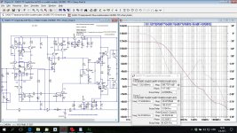
The attached shows the result of a reworked compensation scheme to accommodate 22k & 820 Ohms in the FB path. I think you know already why these two are interesting numbers?
Compared with your approach in #632, due primarily to these higher values, HF performance is reduced very slightly by .1~ ppm.
The arrangement of compensation components to produce this result are notably dissimilar to #632 and are also somewhat off the grid of standard TPC, TMC etc.
The power amps and ASPs enclosures are finished now. Next step to upgrade to the OITPC as in post 632.
... in its first incarnation so please accept my belated congratulations on yet another outstanding amplifier which looks like its about to get even better.
The attached shows the result of a reworked compensation scheme to accommodate 22k & 820 Ohms in the FB path. I think you know already why these two are interesting numbers?
Compared with your approach in #632, due primarily to these higher values, HF performance is reduced very slightly by .1~ ppm.
The arrangement of compensation components to produce this result are notably dissimilar to #632 and are also somewhat off the grid of standard TPC, TMC etc.
Attachments
...The attached shows the result of a reworked compensation scheme
You tried to contact me but my mail box was full.
My email address is >Here<
Best wishes
David
... in its first incarnation so please accept my belated congratulations on yet another outstanding amplifier which looks like its about to get even better.
The attached shows the result of a reworked compensation scheme to accommodate 22k & 820 Ohms in the FB path. I think you know already why these two are interesting numbers?
Compared with your approach in #632, due primarily to these higher values, HF performance is reduced very slightly by .1~ ppm.
The arrangement of compensation components to produce this result are notably dissimilar to #632 and are also somewhat off the grid of standard TPC, TMC etc.
Could you show what you've changed in the schematic? No, I don't know why 22k & 820 values are important, I think that is better to have lower impedance FB network.
Thank you...
... e-mail request sent.
With best regards,
Ian
... e-mail request sent.
With best regards,
Ian
This is still a work in progress...
...to determine final values against likely parasitic strays and to confirm stability with the new inner loop.
The 2 Ohm resistor on the left is part of that effort. It connects before the FB network; after the output of the Tian probe.
I would be pleased to hear any critique you may have of this approach.
I tend to agree with you that lower FB values are generally preferable and indeed sometimes can be safer. However, you have used these same values in previous designs and again in your 'cold buffered' differential input arrangement as seen here.
From study of that method I note that the overall amplifier performance is quite dependant on the quality of the output of the cold buffer. In this case higher FB values are beneficial because it then has less 'work' to do.
For a very high performance amplifier such as the one in this thread. In order to obtain balanced operation by cold buffering do you think it would need to have a FET based input or would a BJT one provide a sufficiently good match?
Could you show what you've changed in the schematic? No, I don't know why 22k & 820 values are important, I think that is better to have lower impedance FB network.
...to determine final values against likely parasitic strays and to confirm stability with the new inner loop.
The 2 Ohm resistor on the left is part of that effort. It connects before the FB network; after the output of the Tian probe.
I would be pleased to hear any critique you may have of this approach.
I tend to agree with you that lower FB values are generally preferable and indeed sometimes can be safer. However, you have used these same values in previous designs and again in your 'cold buffered' differential input arrangement as seen here.
From study of that method I note that the overall amplifier performance is quite dependant on the quality of the output of the cold buffer. In this case higher FB values are beneficial because it then has less 'work' to do.
For a very high performance amplifier such as the one in this thread. In order to obtain balanced operation by cold buffering do you think it would need to have a FET based input or would a BJT one provide a sufficiently good match?
Attachments
...to determine final values against likely parasitic strays and to confirm stability with the new inner loop.
The 2 Ohm resistor on the left is part of that effort. It connects before the FB network; after the output of the Tian probe.
I would be pleased to hear any critique you may have of this approach.
I tend to agree with you that lower FB values are generally preferable and indeed sometimes can be safer. However, you have used these same values in previous designs and again in your 'cold buffered' differential input arrangement as seen here.
From study of that method I note that the overall amplifier performance is quite dependant on the quality of the output of the cold buffer. In this case higher FB values are beneficial because it then has less 'work' to do.
For a very high performance amplifier such as the one in this thread. In order to obtain balanced operation by cold buffering do you think it would need to have a FET based input or would a BJT one provide a sufficiently good match?
It's clear that you know your work. You use more FB loops and quite complicate compensation, but THD is marginally different. In my simulation I used quite low value caps, and you even get lower. In real amp I would use a bit more robust compensation to lower PCB layout influence.
You can use BJT in input LTP, just need to change emitter (source) degeneration.
Regarding NFB impedance I used advantage of fet LTP and used lower FB impedance, as there no need to match input and FB side impedance. In case you use BJT this match is quite important to keep output DC offset low.
You have seen 820/22k FB network in my CFA/VFA version where the NFB network is not referenced to the ground but virtual not perfect ground formed by cold (-) input buffer, and that was best compromise impedance/THD wise.
...The 2 Ohm resistor on the left is part of that effort. It connects before the FB network; after the output of the Tian probe.
I would be pleased to hear any critique you may have of this approach.
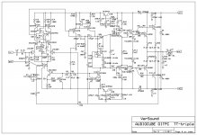
Damir knows the rest of the circuit but for anyone else it would save time if you simply showed the whole circuit rather than small pieces.
Best wishes
David
Last edited:
Duly noted...
... point taken. Please accept my apology for interpreting Damir's request perhaps a little too literally.
As an aside from the values published please could you offer any view on whether the method shown seems theoretically sensible?
Damir knows the rest of the circuit but for anyone else it would save time if you simply showed the whole circuit rather than small pieces...
Could you show what you've changed in the schematic? ...
... point taken. Please accept my apology for interpreting Damir's request perhaps a little too literally.
As an aside from the values published please could you offer any view on whether the method shown seems theoretically sensible?
As an aside from the values published please could you offer any view on whether the method shown seems theoretically sensible?
Sure, once I can see the whole circuit to form a view
")
Best wishes
David
Thank you...
... for your kind words and considered responses.
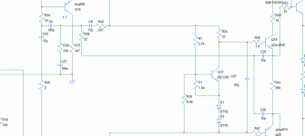
After further rework the circuit now has a degenerated BJT LTP. Off to the left is a servo and cold buffer.

Following an approximate analysis for strays and taking your advice into account the new compensation is now more effective and resilient.

The THD performance is still remarkably good and due to the high quality of the cold buffer is almost entirely unaffected by balanced or single ended connection. The relevant numbers are in each image filename.


Do you think 56 Ohms is sufficient degeneration for the LTP and would you have any concern that the ULGF is still ~2.7MHz but now with 22k & 820 in the FB path?
It's clear that you know your work. You use more FB loops and quite complicate compensation, but THD is marginally different. In my simulation I used quite low value caps, and you even get lower. In real amp I would use a bit more robust compensation to lower PCB layout influence.
You can use BJT in input LTP, just need to change emitter (source) degeneration.
Regarding NFB impedance I used advantage of fet LTP and used lower FB impedance, as there no need to match input and FB side impedance. In case you use BJT this match is quite important to keep output DC offset low.
You have seen 820/22k FB network in my CFA/VFA version where the NFB network is not referenced to the ground but virtual not perfect ground formed by cold (-) input buffer, and that was best compromise impedance/THD wise.
... for your kind words and considered responses.
After further rework the circuit now has a degenerated BJT LTP. Off to the left is a servo and cold buffer.
Following an approximate analysis for strays and taking your advice into account the new compensation is now more effective and resilient.
The THD performance is still remarkably good and due to the high quality of the cold buffer is almost entirely unaffected by balanced or single ended connection. The relevant numbers are in each image filename.
Do you think 56 Ohms is sufficient degeneration for the LTP and would you have any concern that the ULGF is still ~2.7MHz but now with 22k & 820 in the FB path?
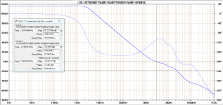
I used my own type of compensation in my CFA amps, parallel TPC, one around VAS and one from the output too, I called it OITPS (output included TPC).
It showed some advantage over TMC, more PM and GM.
I decided to try it in my VFA TT amp so here it is.
Simulation showed quite good result and I went to the practical implementation. First attempt showed some oscillation, and it was resolved by moving Miller compensation from the drivers to the pre drivers (triple is notorious for instability).
Here is the schematic and simulated Loop Gain. The modified amp is playing now, it looks very stable and nice sounding.
So far so good.
Attachments
Nice. So about 30% compensation from output, 70% compensation from VAS output.
I choose it by simulation to get good Phase and Gain margin. Here the OPS is triple and more sensitive to self oscillation. In my CFA I used simpler OPS, only divers and output MOSFETS., and there was possible to use almost fifty fifty compensation.

Congrats!
Hi Damir,
congratulations on your achievements in compensation scheme (post #623), build (post #635) and sound quality (post #653)!
I will probably build a smaller, completely different amp with comparable distortion performance at low to medium power -- with one notable difference: your high-frequency spectrum above some 100kHz is really clean (sim of asc in post #634), while my circuit will produce remarkable noise.
You report some sound improvements with the last design step. Puzzling again and again: how can one hear these small differences? Edmond Stuart reports on his Web page listening tests, where some listeners complained about certain treble harshness in one stereo channel. This then could be traced back to a different small compensation capacitor in this channel.
I can talk of similar experience with my ppm-performance design (low-power, nested MC amp with many, many stages ;-) with respect to small comensation or power supply details, e.g. snubber circuits at rectifiers.
So, my question is: You reported certain small, but clear sound quality progress over the design steps. If one rules out, that only those tiny THD figures determine sound quality: Do you have some hint or suspicion, which other reasons for the improvements one could take into account?
Congrats again and happy listening,
Matthias
PS. Some notable experts like Bob Cordell talk of clipping behaviour. Cannot really believe that; differences already show up at quite low listening levels.
Last edited:
- Status
- This old topic is closed. If you want to reopen this topic, contact a moderator using the "Report Post" button.
- Home
- Amplifiers
- Solid State
- ThermalTrak+TMC amp