Now dream up your own variations and try them. Rcheat is one just one possibility which my tumor and I invented in ten seconds. How about the Teddy Pardo resistor to ground? How about driving the output transistor's base with an actual class AB push pull amplifier that includes emitter resistors and a VBE multiplier set at optimal bias? How about X and Y and Z?
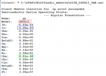
I invite you to calculate it yourself. Just be sure your calculations are performed at Ice = 0.5 amperes, on a PNP whose fT = 50MHz.Cbe calculated to be 61nF ... That seems very high.
Or if your semiconductor physics is a bit rusty, there may be a way to get LTSPICE to print its internally-computed small signal capacitance cbe; perhaps a 15 minute romp through the online Help pages would reveal it.
Or maybe you can devise a clever test circuit that unambiguously measures cbe directly. Then plop it on your protoboard and measure away (or plop the measurement circuit into LTSPICE and simulate away).
Cbe calculated to be 61nF ... That seems very high.
Sure enough, there is such a way; see green box below. I simulated using the spice model from ON Semiconductor's website; apparently its fT at this operating condition is 40 MHz rather than 50 MHz.... there may be a way to get LTSPICE to print its internally-computed small signal capacitance cbe; perhaps a 15 minute romp through the online Help pages would reveal it
_
Attachments
Now dream up your own variations and try them. Rcheat is one just one possibility which my tumor and I invented in ten seconds.
Actually it does make a significant improvement depending on the load scenario (e.g.when the base load is significant such as 0.5->1.0->0.5).
What I am most puzzled about at the moment is that I cannot replicate the Darlington results I got in the third pic here which led me down the Sziklai path rather than Darlington - even when I revert everything to reflect the circuit in the image in that post. Very odd. The Darlington would (now) appear to be the solid outperformer and the push-pull driver can help a good deal.

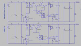
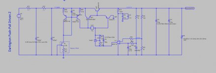
Some people prefer the hybrid NJFET+NPN Darlington topology. Instead of the standard Darlington with emitter follower driving emitter follower, it has a source follower driving an emitter follower. An example from the "SuperTeddy" regulator is attached. {BTW: notice the subtlety of resistor R6 -- usually it would be connected to the emitter of Q4 rather than to ground. Why has Teddy Pardo done it this way instead?}
Now dream up your own variations and try them. Rcheat is one just one possibility which my tumor and I invented in ten seconds. How about the Teddy Pardo resistor to ground? How about driving the output transistor's base with an actual class AB push pull amplifier that includes emitter resistors and a VBE multiplier set at optimal bias? How about X and Y and Z?
I've been tinkering with some options, but none have proven better from a transient perspective than a simple Darlington with 100R resistor from pass transistor base to Vout.
I believe that Teddy Pardo's resistor to ground rather than Vout is simply to get much greater current flow through it (greater dV) and hence drain the Cbe faster. If I route the simple Darlington 100R resistor to GND rather than Vout the circuit behaves very, very much like the push-pull driver configuration where a PNP driver shunts Cbe to GND. It would seem the Pardo configuration achieves basically the same result with less complexity.
A push-pull driver with resistor from pass transistor base to Vout doesn't really get the chance outperform the simple Darlington configuration (with resistor from pass transistor base to Vout) by much if anything. Perhaps the PNP driver to ground doesn't get turned on quickly enough to make a big difference.
Choosing, with respect to transient response, between a push-pull driver or base resistor to GND configuration versus a simple Darlington with base resistor to Vout would seem to be a 'choose your poison' decision. The former are faster to normalise Vout, but with greater overshoot. I'm not sure - based on an eyeball integration - that either has considerably lower overall Vout error.
(I've just been using two 1N4148 to generate the is voltage in the push-pull driver configuration.)
Attachments
Your analysis of Teddy Pardo's mystery resistor, matches mine. Which probably means we're both wrong!
I think it might easily be possible that these subtle-seeming variations, have a not-subtle effect upon the open loop gain and phase. In other words, the different variations might be operating at different amounts of phase margin, and THAT might be the explanation for different amounts of overshoot. So the fairest possible comparison might require you to first jiggle with tenths of picofarads up and down, to get the same phase margin for each variant, before simulating in the time domain.
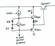
And before you ashcan the push pull forevermore, at least try it with a proper class A bias network. Choose a bias current I0 that you can live with (I suggest 15mA or thereabouts), then choose emitter resistor Rx so that (I0 x Rx) = 26mV. Which means Rx is in the neighborhood of 1.7 ohms. Leave Ry=1.0K and adjust Rz until the collector current of Qpush equals your chosen value I0. Voila, perfect class A operation.
_
I think it might easily be possible that these subtle-seeming variations, have a not-subtle effect upon the open loop gain and phase. In other words, the different variations might be operating at different amounts of phase margin, and THAT might be the explanation for different amounts of overshoot. So the fairest possible comparison might require you to first jiggle with tenths of picofarads up and down, to get the same phase margin for each variant, before simulating in the time domain.
And before you ashcan the push pull forevermore, at least try it with a proper class A bias network. Choose a bias current I0 that you can live with (I suggest 15mA or thereabouts), then choose emitter resistor Rx so that (I0 x Rx) = 26mV. Which means Rx is in the neighborhood of 1.7 ohms. Leave Ry=1.0K and adjust Rz until the collector current of Qpush equals your chosen value I0. Voila, perfect class A operation.
_
Attachments
Your second paragraph may well be correct and I will spend some more time looking at this.
I did quickly compare my simple push-pull configuration with the Class A bias version you depicted above. They're both very similar from a transient perspective, perhaps because the simple version has a good deal of current flowing through Qpush: +60mA (with +50mA being dumped to GND via Qpull).
With an MMBT6429 for Qpush, what might be a good component choice for Qpull? Another BC807-40?
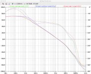
The other thing I want to investigate further is why the Sziklai shows a much lower output impedance even at low frequencies (65.6u versus 18.5u at 1kHz).
I did quickly compare my simple push-pull configuration with the Class A bias version you depicted above. They're both very similar from a transient perspective, perhaps because the simple version has a good deal of current flowing through Qpush: +60mA (with +50mA being dumped to GND via Qpull).
With an MMBT6429 for Qpush, what might be a good component choice for Qpull? Another BC807-40?
The other thing I want to investigate further is why the Sziklai shows a much lower output impedance even at low frequencies (65.6u versus 18.5u at 1kHz).
If you want to run 60mA you might need thru hole or DPAK packages. MMBT6429 in SOT-23 is rated 225mW max (!). Find something whose beta at your bias current is near the max, and whose fT at your bias current is good and high. At least make a table of 8 devices' beta and fT, then choose the table entry with highest numbers. You might decide that a super low VCEsat motor driving transistor from Zetex, looks pretty darn good.
Thanks
I didn't mean to imply that I would want to run 60mA. That would seem wasteful/unnecessary.
If you want to run 60mA you might need thru hole or DPAK packages. MMBT6429 in SOT-23 is rated 225mW max (!).
I didn't mean to imply that I would want to run 60mA. That would seem wasteful/unnecessary.
I looked at Table 8.1a and Figure 8.39 in Art of Electronics 3rd Ed. It would seem to me that the NXP BC860 might be a good choice given space constraints. Lower beta at 10-15mA of Ic than the apparently very capable ZTX718 but in a package that suits a board with little free space on the top layer for a through-hole TO92. Good fT as well. Perhaps a noisy choice but then the MMBT6429 sits high in that table also. Do you think it would be a poor selection overall or should I try to make room for the TO92 ZTX718?
Am I right to think that simple current mirror PNPs aren't worth changing (from BC807-40)?
EDIT: I see Table 8.1a refers to the Infineon version rather than the NXP. The former seems harder to source. Mouser just have the B version and list it as EoL. They have the BC857 in C group (also EoL).
Am I right to think that simple current mirror PNPs aren't worth changing (from BC807-40)?
EDIT: I see Table 8.1a refers to the Infineon version rather than the NXP. The former seems harder to source. Mouser just have the B version and list it as EoL. They have the BC857 in C group (also EoL).
Last edited:
I added a 4.7p compensation cap to the Sziklai to give it a modelled UGF roughly the same as the Darlington configurations. There's now little between the transients responses. I am still puzzled by output impedance given there isn't anything obvious to me in the pass transistor data sheet to suggest the difference. I'm not sure now if it is worth changing the board vs just picking up some small caps...
Attachments
The advantage of taping out a revised Sziklai board is, that it will tell you whether or not you truly have understood the mystery of the "slow" transient response (measured vs. simulated), and whether or not your design revisions have fixed it so the new board is no longer "slow".
The advantage of taping out an EF->EF board is, that you'll now have physical boards to measure for all three output stage types (MOS SF, BJT Sziklai, BJT EF->EF) and can see how they compare in reality, rather than in simulation. You'll also have a chance to possibly observe new manifestations of simulation diverging from measurement thanks to new circuits, which would be a new learning experience. If the simulated performances are identical, I'd probably discard the push pull and just load down the first EF with a Teddy resistor to the bottom rail, chosen to set bias current and quiescent power dissipation as desired. This gets rid of two transistors, two resistors, and one trimmer setting.
The advantage of taping out an EF->EF board is, that you'll now have physical boards to measure for all three output stage types (MOS SF, BJT Sziklai, BJT EF->EF) and can see how they compare in reality, rather than in simulation. You'll also have a chance to possibly observe new manifestations of simulation diverging from measurement thanks to new circuits, which would be a new learning experience. If the simulated performances are identical, I'd probably discard the push pull and just load down the first EF with a Teddy resistor to the bottom rail, chosen to set bias current and quiescent power dissipation as desired. This gets rid of two transistors, two resistors, and one trimmer setting.
One thought I had is that the MOSFET scope shots were with a much lower vertical resolution of 50mV per division. It may well have obscured a lot. It can only be resolved by testing it again.
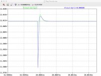
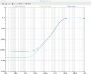
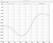
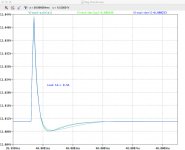
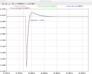
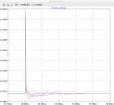
I continued to tinker in sim. It is interesting to look at transients from a lower base level of current. As annotated, the above were transients with loads from 0.5A->1A->0.5A and the bode plot is for load=0.5A. Here is the same work but with load 0.1A->0.6A->0.1A and bode plots with load=0.1A.
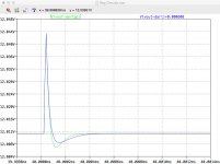
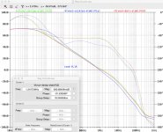
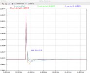
Phase margin for the Darlington configurations expands versus Sziklai. (I kept the 4.7p compensation cap for the Sziklai.) The Sziklai also underperforms significantly when the load comes off. (I should have deleted the red trace darlpp2. It doesn't have a resistor between Qpush and GND and so has high current.) My measurements of the circuit I have built were with minimal 'quiescent current' (stepping c0.5A) which is presumably just the bleeder-LED and op amp quiescent current on the board and whatever load the chop chop box presents when switched to 'off'.
I continued to tinker in sim. It is interesting to look at transients from a lower base level of current. As annotated, the above were transients with loads from 0.5A->1A->0.5A and the bode plot is for load=0.5A. Here is the same work but with load 0.1A->0.6A->0.1A and bode plots with load=0.1A.
Phase margin for the Darlington configurations expands versus Sziklai. (I kept the 4.7p compensation cap for the Sziklai.) The Sziklai also underperforms significantly when the load comes off. (I should have deleted the red trace darlpp2. It doesn't have a resistor between Qpush and GND and so has high current.) My measurements of the circuit I have built were with minimal 'quiescent current' (stepping c0.5A) which is presumably just the bleeder-LED and op amp quiescent current on the board and whatever load the chop chop box presents when switched to 'off'.
Attachments
Last edited:
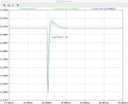
Stepping the Sziklai "base" load: 25mA, 50mA, 100mA, 200mA
(note also the LTspice 'quirk' whereby runs other than the first seem to start 20ns late)
The Darlington configurations have much less variance with base load.
I wonder, real or model imperfections? I guess I will have to take a look at a Darlington based board.
(note also the LTspice 'quirk' whereby runs other than the first seem to start 20ns late)
The Darlington configurations have much less variance with base load.
I wonder, real or model imperfections? I guess I will have to take a look at a Darlington based board.
Attachments
Indeed. There aren't many PNP models shipping with LTspice. The On-Semi D45H11 embedded with LTspice exhibited the same behaviour. I tried a few of the Rohm models and they did not (although I witnessed some bizarre behaviour of delayed transient reactions when stepping the load parameter). I tried a couple of Bob Cordell's models. Both the MJL1302C and NJL1302C models exhibited the behaviour. MJL1302C attached.
I'm puzzled as I would have expected the opposite behaviour given the discussion in post 235 above (lower current => lower Cbe needing to be discharged).
I think I will have a look at what's required to do another board in Darlington config.
I'm puzzled as I would have expected the opposite behaviour given the discussion in post 235 above (lower current => lower Cbe needing to be discharged).
I think I will have a look at what's required to do another board in Darlington config.
Attachments
Then EF->EF it is. With bigger forward drop from in to out, this reduces the opamp's supply voltage and increases the need for a level shifter, which you've already decided to include.
If you're feeling adventurous you could think about using a super high fT device for the initial emitter follower: MPSH10(TH)/MMBTH10(SMD) , 2N5770(TH) , 2SC4082(SMD) , PMBT6428(SMD) , PN2369A(TH)/PSMT2369(SMD) , and so on. Thanks to the modest output current of your regulator, and thanks to the beta of the output transistor, the emitter current of the initial EF can be quite modest. And as long as you pick a device with a common pinout, you'll be able to yank it off the board and replace it with something more orthodox / less frightening, at the first sign of unexpected behavior.
If you're feeling adventurous you could think about using a super high fT device for the initial emitter follower: MPSH10(TH)/MMBTH10(SMD) , 2N5770(TH) , 2SC4082(SMD) , PMBT6428(SMD) , PN2369A(TH)/PSMT2369(SMD) , and so on. Thanks to the modest output current of your regulator, and thanks to the beta of the output transistor, the emitter current of the initial EF can be quite modest. And as long as you pick a device with a common pinout, you'll be able to yank it off the board and replace it with something more orthodox / less frightening, at the first sign of unexpected behavior.
With bigger forward drop from in to out, this reduces the opamp's supply voltage and increases the need for a level shifter, which you've already decided to include.
What data sheet figure is this given by? I was looking at Vce(sat) which is lower for the NPN. In any event, I still have the op amp supplied from Vout.
Thanks. Intuitively (or rather lack thereof) I've been struggling with the concept of an even higher fT device driving a pass transistor of 'modest fT'. I would have thought the fT of the pass device to have been a key constraint. This is because I have been thinking of the driver as controlling the regulation of the pass transistor. In that construct the driver can be as fast as it likes, but if the regulating pass transistor can't 'speed up' then it's a bottleneck.
If there is a connection between the driver and Vout (to load) then I can imagine the regulation being shared by driver and pass transistor (the pass transistor providing the heavy load and the driver doing the fine-tuning). But in the push-pull constructs we've talked about the driver can only deliver via the base of the pass transistor. Can a higher fT driver actually help here? If so then I misunderstand the basic mechanism between driver and pass.
In-to-Out "dropout" voltage is about 2VBE for EF->EF and, now that I think about it, about 2VBE for Sziklai. D'oh! The control terminal voltage (base of the small transistor) is one VBE higher for EF->EF than it is for Sziklai.
One way to think about fT choice is: you want as little phase shift through the (EF -> EF) combo as possible. Of course the big output transistor contributes the lion's share of phase shift, since ruggedness and fT don't go together. So you pick one of the very few possible choices for that transistor and you live with it. The other, smaller, transistor has a lot more possibilities. More opportunities for design creativity or, at least, unorthodox weirdness. Why not see whether anything bad happens (or anything really good happens) if you use a really fast device in this position? At least it will be fun, and possible instructive.
One way to think about fT choice is: you want as little phase shift through the (EF -> EF) combo as possible. Of course the big output transistor contributes the lion's share of phase shift, since ruggedness and fT don't go together. So you pick one of the very few possible choices for that transistor and you live with it. The other, smaller, transistor has a lot more possibilities. More opportunities for design creativity or, at least, unorthodox weirdness. Why not see whether anything bad happens (or anything really good happens) if you use a really fast device in this position? At least it will be fun, and possible instructive.
Last edited:
- Status
- This old topic is closed. If you want to reopen this topic, contact a moderator using the "Report Post" button.
- Home
- Amplifiers
- Power Supplies
- Thermal considerations for Fairchild SDIP bridge rectifiers