Other possibilities might include (a) your measuring instruments are less accurate than TI's; (b) you are not measuring the same thing under the same conditions as TI; (c) you have not connected your instruments to the D.U.T. correctly; (d) TI's datasheet is full of lies; (e) you are measuring a freak, out-of-spec, part; and so on.
Hi
I have two packets of LM2941 each would seem to have been sealed at the factory. Devices in both packets have the same markings however. I replaced the LM2941 on one half of the board with a sample from the other packet. There was no change in behaviour.
While I expect TI to have better equipment I would not expect my scope to be this far off.
Re conditions, I increased Vin to 21V get to Vin=Vout (16V) +5V. No change. Current is within their test range. The unit they use is mV/V. Per which V? Of output?
Re connection, I am merely probing across the terminals of the output capacitor or the terminals of the LM2941 itself. (Probe plus spring to ground.)
I'm planning to test the board with the pre-reg bypassed next.
When with the LM2941 and its output cap removed from the circuit and bypassed I saw the same issue I looked more critically at my test setup.
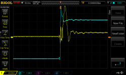
I had been using a relatively long 10" piece of ribbon cable to connect the reg DUT's 4 pole output connector to the chop chop box. I should have known better. I replaced the ribbon cable with a shorter (3 1/2") and thicker wire with Faston connectors from the board's GND X5 Faston tab to the GND tab on the chop chop box and soldered a similar piece of wire from the board's +ve Vout connector pin to the chop chop box (Faston at chop chop box end).
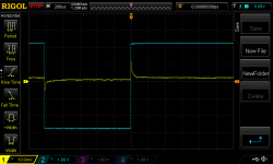
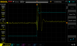
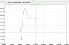
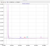
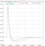
These scope shots are much better. They are from the +ve part of the circuit which still has the LM2941 in place. 18.1Vin. 12.27Vout. I was probing the board's output connector pins.
According to my LTspice model a small compensation cap of 10-22p will assist provide greater phase margin and better dampen the transient response. It costs a bit of high frequency line rejection but may well be worth it.
I had been using a relatively long 10" piece of ribbon cable to connect the reg DUT's 4 pole output connector to the chop chop box. I should have known better. I replaced the ribbon cable with a shorter (3 1/2") and thicker wire with Faston connectors from the board's GND X5 Faston tab to the GND tab on the chop chop box and soldered a similar piece of wire from the board's +ve Vout connector pin to the chop chop box (Faston at chop chop box end).
These scope shots are much better. They are from the +ve part of the circuit which still has the LM2941 in place. 18.1Vin. 12.27Vout. I was probing the board's output connector pins.
According to my LTspice model a small compensation cap of 10-22p will assist provide greater phase margin and better dampen the transient response. It costs a bit of high frequency line rejection but may well be worth it.
Attachments
Last edited:
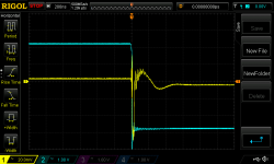
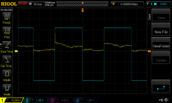
I swapped the chop chop box's frequency setting cap back to 100n. I now have the shortest wires possible from the reg DUT output connector pins (soldered) to the Faston blades on the chop chop box.
Attachments
Maybe now might be a good time to lay out a variant PCBoard using a Darlington rather than a Sziklai CFP as the series pass element? Then you could write out a complete matrix of design topology vs. Load Regulation, Output Impedance, GBW product, Transient Settling Time, and fill in each of the boxes with actual data from your experiences designing and building all three. One matrix for LTSPICE predictions, and another matrix for measured data on real hardware.
Re: "speed"
Among the several possible ways to examine this in LTSPICE simulation, I think one exercise that might produce more light than heat, might be to run the open loop AC analysis simulations of both regulators and compare their unity gain bandwidths. UGB == the frequency at which open loop gain falls to and below 0dB (unity). This frequency depends on many factors, including the microscopic details of Rstability, Cstability, output transistor intrinsic capacitances Cgs, Cgd, Cbe, Cbc, base stopper resistance, gate stopper resistance, impedance ratio between opamp output and (level shifter + output xitor input), and no doubt many more.
But don't do it if you don't believe in it or if you don't quite understand it. Use your own personal definition of "speed" that you do understand and that you do know how to measure. The doubt belongs to you and so does its resolution.
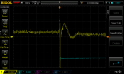
I realise now that what I had commented on with respect to "speed" was a rather different thing. What had attracted my attention was just how long it took the waveforms in post 196 to stabilise (to any degree). Improve the test setup and the observed transient event is sped up a little - post 222. The observed transient event only took 30-40nS here with the Mosfet design. I have tried to see if I saved 'load on' waveforms for the MOSFET design but haven't found them yet.
With respect to UGB, for the MOSFET design modelled UGF was around 1.6MHz. For this Sziklai design it is around 5.3Mhz without a compensation capacitor (and around 2.1MHz with a 10p comp cap).
Last edited:
Best thing for a skeptical person to do is dig the old board out of the junkheap. Measure old board and new board today, on the exact same test setup, using the exact same configuration of input, load, stimulus, and measuring probes. Then simulate both, using the exact same simulation environment for both. Do measurements match simulations? Does human intuition match both? If not, why not?
Are output capacitors identical? ESR / cap value / layout? etc.
Are output capacitors identical? ESR / cap value / layout? etc.
Best thing for a skeptical person to do is dig the old board out of the junkheap. Measure old board and new board today, on the exact same test setup, using the exact same configuration of input, load, stimulus, and measuring probes. Then simulate both, using the exact same simulation environment for both. Do measurements match simulations? Does human intuition match both? If not, why not?
Are output capacitors identical? ESR / cap value / layout? etc.
You are right of course about redoing the tests for the 'old' MOSFET design alongside tests of this new Sziklai-based board. I will try to do so.
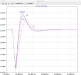
In the interim, I still find a comparison of pics 5 and 7 from the the MOSFET board transient testing with pics 2 and 4 of post 223 above very intriguing.
The tests aren't perfectly comparable because the MOSFET board was being tested with a significant preload. Nonetheless, the timing difference is enormous (circa 7x longer for the 'load-off' waveform).
The same chop chop box (yours) was being used and the output caps for both are the same (2 x Panasonic 667-EEU-FR1E471L). Obviously the board layouts are different with this latest one considerably more compact. (I had meant to create a plane from the +Vout pass transistor to the output connectors rather than the thick trace but never did so. However, -Vout is a plane and the waveforms for both sides of the board were basically the same.)
Another key difference - although I would have thought it less relevant - is that the MOSFET-based board was being tested with mains supply and transformer while input to the Sziklai regulator board was a bench supply of DC just downstream of where the DF06M bridge rectifier would be. Perhaps I am wrong here.
EDIT: the first pic in this post is transient testing of the MOSFET 12V design with no preload and the same chop chop box. Or last 2 pics here.
Last edited:
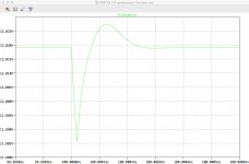
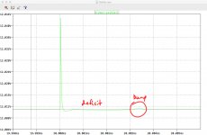
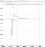
The behaviour noted above seems to me to be intrinsic to a Sziklai configuration - at least with the pass transistor and driver (models) I have used. It is only evident in the "load off" side of the waveform. I understand resistor R23 is intended to help accelerate the turning off of the pass transistor. Altering the value of (or removing) R23 in simulation affects both the load on and load off waveforms. It also shifts the 'bump' I noted above. A lower resistance value leads to less dampening of the "load on" waveform but a faster return to desired Vout when the load turns off (again with less dampening). See sim results. It certainly begs the question as to what the optimal value is (trade off dampening for faster return to Vout) and whether a better solution exists. The load off events takes several micro seconds while the load on is considerably faster.
Attachments
Congratulations for doing a bit of detective work in simulation! It seems likely that the delayed voltage bump on the output will appear on other nodes and/or as a bump in the current through one or more circuit branches. It may be possible to deduce what the root cause might be.
Substituting other transistors (which means: other transistor simulation models) might shed some light on whether this topology always exhibits has behavior X, or whether it only happens with some transistor types but not others. If the latter then you have the uncomfortable task of deciding which models you trust most and which models you trust least, and justifying to yourself those choices.
As for R23, I think from a philosophical perspective, I would probably want to ensure that the PNP transistor never turns off, even with the lighest possible load current. So I would probably arrange for a couple dozen mA to flow at all times, even with the load disconnected, and make sure that at least 1/6th of that amount, comes from the PNP.
Last edited:
I will keep at it. It is not apparent in my MOSFET-based model and I have already tried substituting different Spice models/transistors for Q7 and Q9 (as well as changing the level shift configuration to match the MOSFET-based model). The behaviour was there with all 'variants' I tried so far. I also wondered if the current source (model) was to blame as this differs between the two models (J109 n-channel with source resistor here versus MMBF5461 p channel with gate tied to drain in the MOSFET-based model). When I looked at the current through Q5's collector I saw these delayed bumps in the waveform. But replacing the current source part of the circuit with an ideal 10mA current source still displayed the same behaviour in Vout.
As for sizing R23, I had based the 187R value on reading The Art of Electronics (latest edition). I will look again at the text. In modelling, a much smaller value, e.g. 50R, leads to more overshoot to the downside but next to no "bump" and a faster normalisation of Vout.
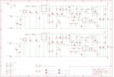
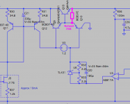
I have attached my Spice model for the curious. The relevant model file is Sziklai.asc. (The pre-reg components can be ignored as they've been 'wired out of operation'.)
EDIT: I realised I had picked another On-Semi model D45H11 when trying a different pass transistor and observing the same behaviour. A bunch of other models threw the circuit into oscillation. Now I tried some more and found that those non-On-Semi models which didn't exhibit oscillation did not have the "bumps". Now the conundrum, model versus real life. I will take another look at the circuit with scope.
As for sizing R23, I had based the 187R value on reading The Art of Electronics (latest edition). I will look again at the text. In modelling, a much smaller value, e.g. 50R, leads to more overshoot to the downside but next to no "bump" and a faster normalisation of Vout.
I have attached my Spice model for the curious. The relevant model file is Sziklai.asc. (The pre-reg components can be ignored as they've been 'wired out of operation'.)
EDIT: I realised I had picked another On-Semi model D45H11 when trying a different pass transistor and observing the same behaviour. A bunch of other models threw the circuit into oscillation. Now I tried some more and found that those non-On-Semi models which didn't exhibit oscillation did not have the "bumps". Now the conundrum, model versus real life. I will take another look at the circuit with scope.
Attachments
Last edited:
As for R23, I think from a philosophical perspective, I would probably want to ensure that the PNP transistor never turns off, even with the lighest possible load current. So I would probably arrange for a couple dozen mA to flow at all times, even with the load disconnected, and make sure that at least 1/6th of that amount, comes from the PNP.
1/6th? When I add the bleeder resistor to LED to the model above and insert 187 for circuit R23 I get 24.9mA of quiescent current of which 21.4mA is coming from the PNP.
It occurs to me that it might be worthwhile to calculate the RC timeconstant at the base of the PNP.
If the PNP is delivering 500mA and the load current suddenly switches to ~ zero mA, its base-emitter capacitance must be discharged by the base-to-emitter resistor R23.
Fairchild's datasheet says D45H11's fT is 40MHz at 500mA; Central Semiconductor's says 50MHz. Cbe = gm / (2 * pi * fT) and gm = 500/26 = 19 Siemens. Thus Cbe = 61 nanofarads. If R23 = 187 ohms then the RC timeconstant at the base is 11.4 microseconds. That seems awfully slow for a circuit that is hoping to have a bandwidth of a Megahertz.
Calculations such as these may be the motivation for Sparkos Labs to use a push-pull driver on the base of their output (series pass) transistor:
The pass transistor is bi-directionally driven by a push pull emitter follower to yield the best transient response possible. Bi directional drive eliminates the long trailing edge that is present in the transient response of many voltage regulator designs that occurs when the load stepps from high current back down to low current.
I never could figure out the push-pull driver configuration (see here) and had dropped it. I wasn't able to apply discussions in texts which related to amplifiers with symmetrical output transistors to this situation of a single pass transistor. Worse, I had trouble applying my feeble fluff at the push-pull darlington model to a Sziklai push-pull. 
Last edited:
Yes the push pull's job is to drive the base of the final, big mother pass transistor. This is easier to do when the big mother transistor is an emitter follower and harder to do when the big mother transistor is a common emitter amplifier with output taken from its collector.
I wonder if you could deliberately undersize the bias voltage "V5" so that V5 < (VBE_q9 + VBE_q10), guaranteeing that there is no possibility of Q9 and Q10 being on at the same time. Then make up for that by providing a cheater resistor Rcheat. Now when the output load current falls to zero, Rcheat does the first little part of discharging the output transistor's base-emitter capacitance. Then after the opamp slews its output a few hundred millivolts, Q10 turns on and honks out LOTS of discharge current.
Now you can make V5 a diode and a half (less than two VBEs). Or a silicon diode plus a schottky diode. Or a VBE multiplier circuit set to 1.66*VBE.
_
Attachments
Cbe calculated to be 61nFIt occurs to me that it might be worthwhile to calculate the RC timeconstant at the base of the PNP.
If the PNP is delivering 500mA and the load current suddenly switches to ~ zero mA, its base-emitter capacitance must be discharged by the base-to-emitter resistor R23.
Fairchild's datasheet says D45H11's fT is 40MHz at 500mA; Central Semiconductor's says 50MHz. Cbe = gm / (2 * pi * fT) and gm = 500/26 = 19 Siemens. Thus Cbe = 61 nanofarads. If R23 = 187 ohms then the RC timeconstant at the base is 11.4 microseconds. That seems awfully slow for a circuit that is hoping to have a bandwidth of a Megahertz.
Calculations such as these may be the motivation for Sparkos Labs to use a push-pull driver on the base of their output (series pass) transistor:
The pass transistor is bi-directionally driven by a push pull emitter follower to yield the best transient response possible. Bi directional drive eliminates the long trailing edge that is present in the transient response of many voltage regulator designs that occurs when the load stepps from high current back down to low current.
That seems very high.
I wonder if you could deliberately undersize the bias voltage "V5" so that V5 < (VBE_q9 + VBE_q10), guaranteeing that there is no possibility of Q9 and Q10 being on at the same time. Then make up for that by providing a cheater resistor Rcheat. Now when the output load current falls to zero, Rcheat does the first little part of discharging the output transistor's base-emitter capacitance. Then after the opamp slews its output a few hundred millivolts, Q10 turns on and honks out LOTS of discharge current.
See attached. I've amended things like the current source to conform with the latest circuit. (Curiously, I don't see the delayed bump behaviour even in the circuits using the same On-Semi pass transistor. I will investigate further.)
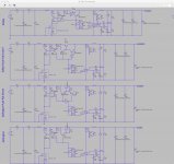
There still appears little difference between the push-pull Darlington (with Rcheat) and the regular Darlington, each of which outperforms the Szilkai configurations (my Sziklai push-pull doesn't seem to work at all). This contrasts with my previous examination and I need to investigate why. I've included a zip of the relevant model files as the circuits image is perhaps hard to see. The relevant file is Reg Circuits.asc.
Attachments
Last edited:
(Curiously, I don't see the delayed bump behaviour even in the circuits using the same On-Semi pass transistor. I will investigate further.)
Seems to be related to assuming the load returns to zero (rather than a lower positive number). The model immediately above steps the load from 0.5 to 1A and back while previously I had been stepping the load from 0 to 0.5A and back.
- Status
- This old topic is closed. If you want to reopen this topic, contact a moderator using the "Report Post" button.
- Home
- Amplifiers
- Power Supplies
- Thermal considerations for Fairchild SDIP bridge rectifiers