Yes I would never argue against gate stoppers with DMOS, especially in TO-220 packages! And I recently had a 2N7000 (TO-92) take off even though it had about 400 ohms in one of the leads --- but there was a fair amount of inductance in the gate (this was not a tight layout, I was using it to drive a string of IR emitters) in photovoltaic optoisolators.Yes, most of the time gate stoppers are not necessary but havoc happened to Calvin so in a privat communication i recommended the gate stoppers. I did not get a response so far if that solved the problem. With depletion Mos Fets like DN2540 it is mandatory or they get so hot that they burn.
If one can get away without them for the lower speed process 51 parts like the 4391, it appears from sim that using them in the cascoded voltage follower leads to a small increase in distortion, so they may be worth losing.
BTW, has anyone used the smaller depletion-mode DMOS part, the DN1509? It looks promising, with a still-high 90V breakdown and lower capacitances.
Although with tube circuits the low frequency noise of the tube will almost always dominate, as triode plate loads or in other highish-voltage applications, I don't like to rely on the uncertain and unspecified amount of low-frequency noise using the DMOS as the lower device. I will say however that DMOS has gotten so much better in the many years since introduction, that some are quite acceptable, despite the low frequency noise. The noise corner frequency keeps going down --- it would be interesting to graph the typical descent over the years.I use other small depletion Mos Fets for cascode CCCS´s. I forgot the part number but up to 50mA they work with high voltage to burn. Usually only one of them has to take the high voltage.
At Walt Jung's suggestion I did get some DN2540s in TO-92 and tested them for noise, which was not as bad as I had feared but still high compared to good JFETs. However as a cascode device for low-pinchoff JFETs they will contribute negligible noise, and the high voltage capability, within the limits of device dissipation, is very convenient.
Try P channel laterals. I friend of mine made an MC input stage with two in parallel that got down to 0.3nV/qHz. He uses a special way of tackling the 1/F noise though. Willy Sansen says that in his book " Analog Design Essentials ". P - channel lateral Mos Fets are excellent for low noise audio.
Interesting. I'd love to learn more, if you can dig up the part numbers.Try P channel laterals. I friend of mine made an MC input stage with two in parallel that got down to 0.3nV/qHz. He uses a special way of tackling the 1/F noise though. Willy Sansen says that in his book " Analog Design Essentials ". P - channel lateral Mos Fets are excellent for low noise audio.
Wayne of Pass Labs just sent me a couple of the big Interfet parts, which also claim a typical e sub n of 0.3nV/sqrtHz. Someone said that the chip inside of the singles is in fact a dual that they use for another part. That must be one large chip!
This does not lend to parallel symmetric though, the complimentary 2SK1058 is quite noisy.
What an irony, now we have a P-Channel but not an N-Channel. The world upside down !
Production will have to be moved to Australia.
(my friends there hate to it being referred to as "down under"
") )
)Production will have to be moved to Australia.
(my friends there hate to it being referred to as "down under"
Dunno what you're talking about - we're at the top, see here:
The Upsidedown Map Page - World Maps with South at the Top
Attachments

Dunno what you're talking about - we're at the top, see here:
The Upsidedown Map Page - World Maps with South at the Top
My friend DHC wanted to know where the earth was --- above or below the Galactic Plane.
WTF? Who defines the up and down of that to begin with??
My friend DHC wanted to know where the earth was --- above or below the Galactic Plane.
WTF? Who defines the up and down of that to begin with??
someone who wants to map it I guess
someone who wants to map it I guess
I guess it has to do with the "handedness" of things defining a rotation axis. That reminds me of a professor I know who said he went through an E&M final as a student writing with his right hand and using his left hand for vector cross-product guidance (the so-called "right-hand rule"), thus getting a bunch of signs wrong.
Hi,
bcarso, You are right. The gate resistors of the cascode JFETs are not needed in the combination of LSK389C and MMBF/SST4391. The pin layout of the LSK389 SOIC-8 and the SOT-23 allows for tight direct connections. You won´t even need a 0-Ohm resistor to bridge a trace. Gate stoppers might be required with other transistor combinations though.
Patrick, the DAO sure is the most powerful, but it is the most complex and is it unconditionally stable? I had already oscillation problems with the much simpler Borbely buffer (CCS, modulated via a upper drain´s resistor and a RC-Gate-Network to the lower JFET). I assume the DAO could be even more prone to instability.
The third Buffer of my post -btw. would ´cascoded Sziklay pair´ be a correct naming(?)- is compensated for by only the small caps C1 and C2.
It may have been overlooked, but all parts of all three buffers are SMDs, allowing for small, compact footprints and all three may be DC-coupled.
The first two circuits are best used with load impedances >10kOhm and Zload should not drop below 1kOhm. The third circuit is best between 10kOhm and 300Ohms. Either with MOSFETs or bipolars, running on ~50mA bias current, it can drive 300Ohms to 3Vrms, which is sufficient for home and studio line level circuits.
Joachim, the probs I had were with a simple ccs loaded Source-follower (like the first in my post). It used BF244C or BF246A and input AC-coupling of the stage with a Gate resistor of >1MOhm. It eventually suffered from serious dc-offset (input and output were driven into one of the supply lines) and fatal destruction.
In our correspondence You assumed heavy oscillations as reason and suggested the use of Gate stoppers. I later found out that the JFETs didn´t oscillate, but latched-up, due to rising Gate leakage, which itself was affected by temperature, Vds and the high valued Gate resistor (a self amplifying effect). Reducing the value of Rgate and changing to different JFETs solved the prob.
jauu
Calvin
Last edited:
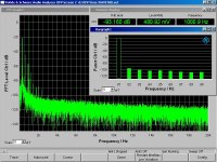
Another update, showing THD measurements.
We are not totally happy with the PSRR and DC drift, even if they are quite OK.
So we are currently working on an improved version to solve both of these problems.
As soon as we have test results, we shall let you know.
The bad news for the new version is, you would need 5 pairs of matched 2SK246/2SJ103 and 1 pair of 2SK170.
Patrick
Attachments
- Home
- Source & Line
- Analog Line Level
- The XCEN -- Balanced to Single Ended Converter