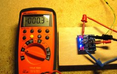
So test results of both prototypes as follows. It could not have gone more smoothly.
The circuit uses pre-calculated values of potential divider of the TL431s to account for the different Vgs of the Zetex MOSFETs.
Power supply was my lab supply, +/-24V, no on-board caps on the rails.
Supply cables are about 1m long.
On power up, DC offset was about 100mV, and no oscillations were observed with inputs shorted to Gnd.
The DC offset went down to about 30mV after 3 minutes.
Once it stabilised, the offset value was converted (by calculation) to trimming resistor values.
These were then soldered onto the PCB (1206 SMD resistors).
After trimming, DC offset at power up is now about 50mV, but dropping to less than 3mV in 5 minutes.
Within the next 20 minutes, it fluctuates between +/-5mV.
This corresponds to an offset current of 2.5µA at a total bis of 40mA for the entire circuit.
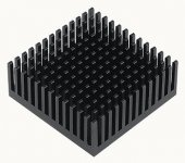
The TO92 JFETs and the E-line MOSFETs are at about 50°C at steady state, even though dissipation is only 100mW or so.
I am very confident that this can be improved by a factor of two by thermally coupling all devices to a heat spreader.
This we already planned from the start, but we wanted to test first before getting it manufactured, as it does add cost.
On top of the spreader (and the top of all FETs), will be mounted a CPU type heatsink of 45x45mm.
This will not only allow the different devices to track each other thermally.
It will also lower the overall temperature with the aid of the large heat sink.
And the thermal mass of the spreader and the sink will even out fluctuations with time.
As such, I personally do not think a servo is necessary, even though it can be added easily on an additional PCB underneath.
I can even live with 5mV as is.
The rest of the test is essentially same as Joachim, and same on both of my prototypes.
Bandwidth is -3dB, 2MHz. Perfect 10kHz square waves.
Gain is as predicted but can also be trimmed easily by adding a trim resistor.
Distortion is much lower than 90dB on 2Vrms, and beyond my measurement capability.
So that would have to wait till I get my hands on an AP again.
We already did a version 2 of the PCB where the left and right channels are mirror images.
And we also added electrolytic caps for the rails on board.
Once we get the thermal management tested, that would be it, as far as I am concerned.
QED.
Patrick
PS
On the DSO plot attached, green is input (functions generator 10KHz Sq), cyan is output.
Vin- was connected to Gnd in this case.
What schematic are you referring to?
Integration with BIII & AckoDAC
This is really good news. You guys never cease to amaze me.
Finally I can use k170/J74 again for a good design.
One request:
Since you are modifying the layout to incorporate the thermal heatsinks, would it be possible to arrange the balance input so it can be connected directly to Buffalo III DAC board by using a 3 pins connector ?
I would like to have the option for connecting directly to AckoDAC as well but the board has different balance output connections than the BIII DAC.
Thanks.
Last edited:
> Finally I can use k170/J74 again for a good design.
The circuit uses 2SK246BL / 2SJ103BL for the front end diff pair, as mentioned in Post #1.
They are much easier to get than 2SJ74.
But of course you can use 2SK170/2SJ74 instead, if you so wish.
The output buffer is a pair of matched 2SK170s, though 2SK246s will also do, but has a somewhat higher Zout.
> Since you are modifying the layout to incorporate the thermal heat sinks,
No Sir. We are not changing the layout for the heat sink.
The heat sink has already been designed months ago that will fit the current layout.
And this is a layout for general application.
3 pieces of twisted wire will allow you easy connections to any balanced output of the preceding circuit.
Patrick
>
No Sir. We are not changing the layout for the heat sink.
The heat sink has already been designed months ago that will fit the current layout.
And this is a layout for general application.
3 pieces of twisted wire will allow you easy connections to any balanced output of the preceding circuit.
Patrick
Ok. That should not be too big of a problem.
Is there going to be a group buy for this ?
The heat sink has already been designed months ago that will fit the current layout.
Any chance to see the layout of the sinks?
I love the tiny CEN/SEN sinks and I'm sure the (more complex?) XCEN sinks will be equally beautiful
")
Cheers,
nic
It is a modified Fischer ICK PGA 17x17, with a few holes for screws and wiring.
Not so romantic as the Dual JFET heat sinks, but lower costs and I expect to be very effective.
Have not decided whether to allow the LEDs to shin through by drilling extra holes or not.
First version will not have those fancy things. It has to work first.
I don't want to spoil things by using a servo.
The performance is already so outstanding as is ......
Patrick
Attachments
Last edited:
Hi,
Patrick, are You sure that the simple JFET-Buffer will be "THD-transparent".
It will at least require easy high-Z loads.
Attached are variations which may be superior alternatives under more difficult conditions, though at the cost of increased complexity.
jauu
Calvin
Patrick, are You sure that the simple JFET-Buffer will be "THD-transparent".
It will at least require easy high-Z loads.
Attached are variations which may be superior alternatives under more difficult conditions, though at the cost of increased complexity.
jauu
Calvin
Attachments
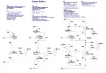
What are the resistors in series with the 4391 gates for?Hi,
Patrick, are You sure that the simple JFET-Buffer will be "THD-transparent".
It will at least require easy high-Z loads.
Attached are variations which may be superior alternatives under more difficult conditions, though at the cost of increased complexity.
jauu
Calvin
The PCB will allow you to take the output directly at the resistor in front of the JFET buffer, if one so wish.
Bear in mind that this is a line-level circuit and not designed to drive 600 ohm loads.
More like 5~10k.
One can always add a unity gain buffer of any sort.
There is none more powerful than the DAO, for example (power amps excluding).
If I am not wrong the resistor at the 4391 gate is meant to be used as a gate stopper.
But Calvin should answer that one.
Patrick
That bootstrapped cascode does have a negative input Z characteristic, but I find that usually the source Z has enough C to compensate for it. I've never found oscillations in tight layouts with those exact components in through-hole for the second circuit shown. These were hand-wired on ground plane perf board.Yes, it is against oscillation although it seems odd.
Yes, most of the time gate stoppers are not necessary but havoc happened to Calvin so in a privat communication i recommended the gate stoppers. I did not get a response so far if that solved the problem. With depletion Mos Fets like DN2540 it is mandatory or they get so hot that they burn.
- Home
- Source & Line
- Analog Line Level
- The XCEN -- Balanced to Single Ended Converter