Soulution are the best amplifiers I have heard (by far) but of course this is a subjective matter.
My comment was just a joke because, given the complexity of the amps and judging by the way the Goldmund thread goes, the relevant thread would hit the forum page limit pretty fast. ;p
My comment was just a joke because, given the complexity of the amps and judging by the way the Goldmund thread goes, the relevant thread would hit the forum page limit pretty fast. ;p
Godfrey - Here's a picture for you:
An externally hosted image should be here but it was not working when we last tested it.
Goldmund connects the diodes D2, D5, D4, and D6 slightly different from Hafler, Nelson Pass, etc. This doesn't mean that it's incorrectly connected. Both ways work and serve their purpose. Why did Goldmund chose to connect their diodes that way? Simply because they worked to serve a certain purpose that the Goldmund engineer wanted to implement in the amplifier!!
The reason why a lot of people are having a problem with this is because they're simply audiophiles who are used to cloning Nelson Pass designs. That is what they're familiar with. They're not real engineers. There are no set ways that something can be connected. To find out why Goldmund connected their diodes that way, one would need to test the amplifier and see what happens, otherwise it's all purely a speculation.
Once again, we are trying to clone a Goldmund Mimesis 9.2 amplifier here. Because of narrow mindedness, a lot of people want to change the circuit to what they're familiar with. In that case, please go build the boring $20 Nelson Pass amplifiers.
Furthermore, why do we need 10-20 pages of arguments each time on something as trivial as T6's orientation, or weather to use the small pF capacitors, or how the diodes should be connected? You are building a Goldmund amplifier, that's how they do it. This shouldn't leave any room for argument. If you want to change all these things, please do so. The PCB will need no modifications, it's as simple as rotating the parts and soldering them in reversed. The PCB and the schematic has to be displayed as per original Goldmund. It's up to the individual builders to do their own upgrades (or more than likely failures).
Spind - I'm rude? Have you read the constant attacks in this thread? Your lack of observation skills are not only rude, but also insulting.
Don't you think your being a little harsh on Nelson, his amps and fans of his amps?
I guess the thing about this thread that is a little different to most is that someone is designing a board on your instruction. We call this collaboration when we colaborate we take suggestions from different folk and the thread can go anywhere. You seem to want to control all aspects of this design, but I think the only way to do that on a forum is if its your project.
Perhaps thats why some folk around here appear to be rude, maybe they find you rude?
All I'm saying is this amp may well be great, but chill out and see where this thing goes and consider expert advice, theres plenty of it here.
Good luck.
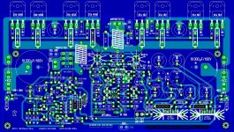
PCB ....rev 3.3
... sorry for delay , I have no much time in this season , so somes changes on board , ofcourse will be negative comments regarding layout . I do my best , I'm stil learning")
Alex .
... sorry for delay , I have no much time in this season , so somes changes on board , ofcourse will be negative comments regarding layout . I do my best , I'm stil learning
Alex .
Attachments
Last edited:
Can wires be run to the pcb or is the pcb only suitable for the new style fets. Or maybe some sort of adaptor pcb is possible?
You'd definitely need an adaptor board, with pads for both the TO3 pins and for the gate resistors.
Wires straight to the output devices is the absolute worst choice.
Something that is no problem with Vertical MOSFETs or with power BJT's, not with Laterals.
Even with solid wires and resistors soldered right at the gates you'll risk spending the next month playing Mikado to stop the thing from oscillating.
... sorry for delay , I have no much time in this season , so somes changes on board , ofcourse will be negative comments regarding layout . I do my best , I'm stil learning
Alex .
Alex, your work is superb and very much appreciated by ALL.
I have have but one question for you that has bugged me from the beginning. WHY you have never changed the width of the power going to the output devices? It has been mentioned many times, by different ones, including myself. It seems so simple from my point of view. Enlighten me and maybe others why you choose NOT to make the traces wider.
This boards input and design from you is without much room for improvement.
It is a joy to see your hard work and tenaciousness.
Your future is bright and we are blessed to see you at the onset of a great career.
Thanks
You'd definitely need an adaptor board, with pads for both the TO3 pins and for the gate resistors.
Wires straight to the output devices is the absolute worst choice.
Something that is no problem with Vertical MOSFETs or with power BJT's, not with Laterals.
Even with solid wires and resistors soldered right at the gates you'll risk spending the next month playing Mikado to stop the thing from oscillating.
Thats my experience too with these fets, no pcb no stable. Wires will never work.
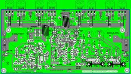
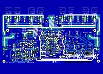
PCB for TO3 finals transistors
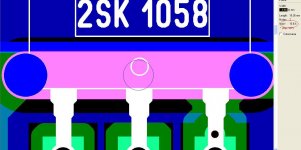
Hi , Krisfr , thanks for the kind words , I do my best how I sed befor . First to make my self clear whay I draw power traces not so width it's because I have 3.5mm width wich support 10.8 A and fuse are rated at 6A current .Solder mask has an tined surface and 2.5 mm trace width ,se picture below .I think problem solved now .I have done this afternon the new revised PCB with TO3 finals transistor 2SK 134 and 2 SJ 49 .
Alex.
Hi , Krisfr , thanks for the kind words , I do my best how I sed befor . First to make my self clear whay I draw power traces not so width it's because I have 3.5mm width wich support 10.8 A
and fuse are rated at 6A current .Solder mask has an tined surface and 2.5 mm trace width ,se picture below .I think problem solved now .I have done this afternon the new revised PCB with TO3 finals transistor 2SK 134 and 2 SJ 49 .Alex.
Attachments
Hi Alex, thank you for your hard work. I will have to say that the previous version of your PCB layout was significantly better and is the one that should be built. The location of capacitors C32/C35 and C33/C36 between the MOSFES is not good. Both of these capacitors have to be located before all MOSFETS. In your last PCB all that was needed was to switch the positions of C32/C35 with C33/C36 and it would have been a perfect board. The amplifier might not even function properly with the current location of these capacitors.
Also, capacitors C30/C29 were in the correct location in the last PCB (regardless of what someone wrote in this thread). They should be as close as possible to T3, T4, T5, and T6.
Also, capacitors C30/C29 were in the correct location in the last PCB (regardless of what someone wrote in this thread). They should be as close as possible to T3, T4, T5, and T6.
Alex!!! You posted this right after I wrote my last post. This latest PCB layout is close to perfection!!!!!
Please take a look at capacitors C33/C36 and make sure they are connected to the trace. The one on the left especially looks to be not connected.
Also, please put C30/C29 next to T3, T4, T5, and T6 and this board will be perfect and flawless!!
I think everyone in the group buy should build this version with the metal can TO3 MOSFETS. They sound significantly better and are readily available (Magnatec BUZ900/BUZ905, BUZ901/BUZ906, Exicon ECF10N16/ECF10P16, ECF10N20/ECF10P20).
Awesome!
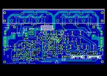
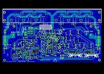
PCB for TO3 revised
.....Krisfr the copper is 35 microns tickness on battom and top side.
I find in the last board design an big mistake , I has connected minus rail to output , now corrected , right picture below .
Alex.
.....Krisfr the copper is 35 microns tickness on battom and top side.
I find in the last board design an big mistake , I has connected minus rail to output , now corrected , right picture below .
Alex.
Attachments
Last edited:
.....Krisfr the copper is 35 microns tickness on battom and top side.
I find in the last board design an big mistake , I has connected minus rail to output , now corrected , right picture below .
Alex.
Ok that is 1 oz.
I suggest 2, but you will get some help from the plating...
The reason why a lot of people are having a problem with this is because they're simply audiophiles who are used to cloning Nelson Pass designs. That is what they're familiar with. They're not real engineers.
Once again, we are trying to clone a Goldmund Mimesis 9.2 amplifier here. Because of narrow mindedness, a lot of people want to change the circuit to what they're familiar with. In that case, please go build the boring $20 Nelson Pass amplifiers.
What a statement.

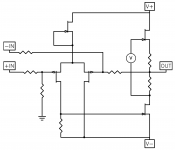
Ok Mr Engineer have a look at the simplified schematic below. If you can build a J2 amp from this schematic (or any other Pass amp for that matter) all cased with heatsinks and transformer for $20. I will happily give you $100 for it. Actually I will happily give you $200 for it.
Make my day.
Attachments
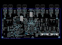
Hi Alex, this latest PCB layout is perfect. I cannot think of a single change. I also carefully compared it with the original schematic and there seems to be no mistakes.
I would like to make one last suggestion... The top of the board has a ground plane. The aluminum metal bracket (where the MOSFETS will be mounted to) will mount on top of this board. This metal part cannot come into contact with the ground plane, because at that point the chassis and the ground plane will be connected and that's no good. One solution is to use an insulator under this aluminum metal bracket. This will require no changes to the PCB.
But another solution (which would make building this amplifier a little easier) is to make a line where the ground plane's metal is missing. Please see the picture below, I drew it in red.
And here's a picture of the Goldmund Mimesis 6 amplifier. You can see on the bottom that the ground plane has a line of missing metal by the metal bracket.
Weather you decide to incorporate this change, or not. I think the board is ready. Can you please generate the Gerber files and send them along with the Sprint files to Bigpanda? Thank you again for everything that you've done
I would like to make one last suggestion... The top of the board has a ground plane. The aluminum metal bracket (where the MOSFETS will be mounted to) will mount on top of this board. This metal part cannot come into contact with the ground plane, because at that point the chassis and the ground plane will be connected and that's no good. One solution is to use an insulator under this aluminum metal bracket. This will require no changes to the PCB.
But another solution (which would make building this amplifier a little easier) is to make a line where the ground plane's metal is missing. Please see the picture below, I drew it in red.
An externally hosted image should be here but it was not working when we last tested it.
And here's a picture of the Goldmund Mimesis 6 amplifier. You can see on the bottom that the ground plane has a line of missing metal by the metal bracket.
An externally hosted image should be here but it was not working when we last tested it.
Weather you decide to incorporate this change, or not. I think the board is ready. Can you please generate the Gerber files and send them along with the Sprint files to Bigpanda? Thank you again for everything that you've done
Last edited:
- Home
- Amplifiers
- Solid State
- The Very Best Amplifier I Have Ever Heard!!!!