.....Krisfr the copper is 35 microns tickness on battom and top side.
Alex.
Hi Alex,
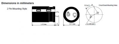
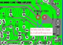
Very nice board. The holes for the big snap-in filter cap is a bit too small - it look like 1.5 - 1.6mm dia. It should be 2mm according to Panasonic datasheet.
BTW, can you change the layout a little bit so that the 6x gate 100R resistors can be mounted under the PCB, just like the 10nF capacitors from D to ground.
The gate resistor should be very close to the gate pin to avoid oscillation.
When the gate resistors are out of the way, you can also move the two 1uF/160V film caps away from the output FETs, then the potential builders can have more clearance for their heatsink bracket.
Cheers, Stanley
Attachments
Sorry, I don't know a simple harmless 4 word sentence like "Try to read them. " could be so irritating to any human being. So I think I should just address anything to everyone, not just anyone in particular from now on.
Back to tech,
I see that the source resistor (0.22ohm) is missing from alex's TO-3 version board. Can 'anyone' (or should I use 'everyone' here, but I think this is going to be a grammatical mistake) please kindly shed some light on this?
Back to tech,
I see that the source resistor (0.22ohm) is missing from alex's TO-3 version board. Can 'anyone' (or should I use 'everyone' here, but I think this is going to be a grammatical mistake) please kindly shed some light on this?
While we are at it. I may as well mention I also have a tektronix and a Le Croy oscilloscpe.
So it better pass the testing, because if it doesn't I will know about it sure enough.
While we are at it, I will as well mention that I also have an oscilloscope (Grundig Oscilloscop G10/13Z), but can not use it. And will never use it because I have just broken it down to pieces

Nagys,
If they are vital to the circuit, no matter how big they are, they have to be there. Just want to make everything sure and make this project right, that's my only aim.
BTW, I am planing to add an extra pad to some transistors so as to make them easier for use with alternatives. Instead of a tripod (as in original), make the legs in-line and with the flat side facing the other way (for the alternatives). It seems that of all the alternatives that you mentioned, they are having a reverse EBC arrangement than the original. I will try documenting them when I get all things ready. It might look a bit crowded with pads but it may be easier for some guys. As long as they know which holes they should be in, that should be OK.
If the 2oz thick copper for the power and output traces is good enough for that width, I will keep them that way. If not, I might attempt to broaden them. Please comment.
Bigpanda - They are not vital and again none of the Goldmund Mimesis amplifiers use them. The only reason they were added by Alex before, was because of someone's suggestion. These resistors are not part of the schematic and shouldn't be used if you're building a faithful Goldmund clone.
In my opinion, the extra pads are not necessary. Also, weather the holes are in a tripod configuration, or in a straight line doesn't make much of a difference either. If anything, I personally prefer the tripod layout, the transistors sit firmer. While in a straight line, you could bend them around easier.
The width of the tracks is perfect. They will never ever reach their 15+ amp rating.
I think that the TO-3 version of the board should be made. If people decide to use the TO-3P transistors, they will still fit. The 2 outer pins of the plastic version transistor just need to be bent 90 degrees to go through the PCB holes.
The source (case) will be connected with a single screw to the PCB.
Daniel
The source (case) will be connected with a single screw to the PCB.
Daniel
They are vital for good current sharing. Other way precise selecting of Mosfets (Vgs treshold and Vgs vs Id) is a must.They are not vital
Last edited:
They are vital for good current sharing. Other way precise selecting of Mosfets (Vgs treshold and Vgs vs Id) is a must.
Then you must buy 100+ , sort them into groups. Even WITH .22R emitter resistors and BJT's, crude matching is recommended. Had an amp with all devices dropping 13mV Re , one dropped 17mV ... guess which one blew ??
OS
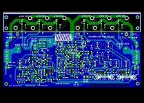
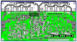
PCB Rev 3.7
Hi Alex,
Thanks for the quick changes.
Can you please double-check the hole size for the 10000uF capacitor? If the picture represent the actual hole size, then they look like 1.5 to 1.6mm diameter and that will not fit the snap-in capacitors (which require 2mm mounting holes). The potential builder cannot drill that out either as the speaker ground is connected to one of the 10000uF cap.
Cheers, Stanley
Attachments
Alternatives
Hopefully we are close to have our PCB for the Golmund clone. From time to time Nagys/Alex/Bigpanda receive questions that will result in changes on the PCB.
Mostly Nagys rejection is in respect to the orginal. That’s ok, but why is it so diffucult to take into account solutions that give alternative options and still satisfy those who want to be faithful to the original.
Let me mention three issues from some of the latest posts:
C31/C34: 30 or 35 mm and holes for snap in.
Source resistors. Do we know if Golmund have matched them or not? Even if they have not:
For those who will feel more comfortable with an opportunity for source resitors, let us have it. We can cut the copper lane between the mounting holes for the source resistors. Or use a bare wire for those who want to bypass.
Eivind Stillingen
Max diameter for C31/C34
Hi Eivind,
I have checked, 35mm diameters capacitors can be installed on the last two PCB version by alexmm.
I think that is up to builder to choose the capacitance - the board can fit anything from 4700uF to 10000uF.
Cheers, Stanley
C31/C34: 30 or 35 mm and holes for snap in.
Eivind Stillingen
Hi Eivind,
I have checked, 35mm diameters capacitors can be installed on the last two PCB version by alexmm.
I think that is up to builder to choose the capacitance - the board can fit anything from 4700uF to 10000uF.
Cheers, Stanley
If the schematic says 4700 why use a higher value? Is it because we know better? After all a higher value can only be better right?
For those wanting to use 1000 watt torroids and big caps consider what ivodonchev points out. The use of the smaller size transformer and capacitor values could be a deliberate design choice.
2. Lowering the +/-80V at output stage down to +/-50V will NOT LOWER the power of the amplifier and will not increase THD. I think that Goldmund's reason to use 80V is probably sonic performance not measurable. At the some time with +/-80V at high power and 4 Ohm load the output mosfets will go out of power range easily. Probably that's why they use not oversized transformers and only 4700uF capacitors because this will give around 73V at high power and low load. This will be a little bit safer for output mosfets.
For those wanting to use 1000 watt torroids and big caps consider what ivodonchev points out. The use of the smaller size transformer and capacitor values could be a deliberate design choice.
- Home
- Amplifiers
- Solid State
- The Very Best Amplifier I Have Ever Heard!!!!