Lee Knatta - What layout mistakes did you point out that are fixed now?
My concern regarding the grounding scheme was in post #861 and my suggestion for changes was in post #863.
Your input was in post #864.
Alex posted the updated PCB layout with my suggested changes (to mimic Goldmund more closely) in post #891.
Nothing you posted in #864 was incorporated. Your contribution is zero. If you continue to lie, I will continue to call you out on it.
Wrong. You lie.Your input was in post #864.

The whole discussion began with post #835.
Do you really want to go through this all again?
I doubt it.Aha! Do you have a photo of the other side so we can see what connects to where? I remember your previous photos doing a good job of settling the T6 argument...... Please see the picture below, they are right between the MOSFETS and the A1 module:
... You can clearly see which sides are marked with the black Cathode ring.
Kidding...
You must be kidding...When you're done, please clone Soulution's gear. That'll be a fun thread.
Attachments
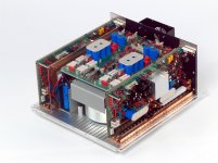
Soulutions amp is almost as ridiculous inside as the Goldmund. Although the electronics is designed industry standard and looks nice instead of cheap and crappy 70's DIY style in the Goldmund amps I wonder how they can dissipate 200W without any reasonable heatsink. Instead they have three thermal junctions to that thick aluminium base plate. What's wrong with the swiss high end audio manufacturers?
However, a good candidate for cloning.
All we need for this project is an audiophool totally clueless but fan of Soulutions Audio who will be the head of Soulutology.
However, a good candidate for cloning.
All we need for this project is an audiophool totally clueless but fan of Soulutions Audio who will be the head of Soulutology.
Although the electronics is designed industry standard and looks nice instead of cheap and crappy 70's DIY style in the Goldmund amps
that is the worst argument ever
industrial design doesnt improve sound as such, on the contrary
nothing wrong with the diy style from the seventies
at least they looked like real amps
Godfrey - Here's a picture for you:
Goldmund connects the diodes D2, D5, D4, and D6 slightly different from Hafler, Nelson Pass, etc. This doesn't mean that it's incorrectly connected. Both ways work and serve their purpose. Why did Goldmund chose to connect their diodes that way? Simply because they worked to serve a certain purpose that the Goldmund engineer wanted to implement in the amplifier!!
The reason why a lot of people are having a problem with this is because they're simply audiophiles who are used to cloning Nelson Pass designs. That is what they're familiar with. They're not real engineers. There are no set ways that something can be connected. To find out why Goldmund connected their diodes that way, one would need to test the amplifier and see what happens, otherwise it's all purely a speculation.
Once again, we are trying to clone a Goldmund Mimesis 9.2 amplifier here. Because of narrow mindedness, a lot of people want to change the circuit to what they're familiar with. In that case, please go build the boring $20 Nelson Pass amplifiers.
Furthermore, why do we need 10-20 pages of arguments each time on something as trivial as T6's orientation, or weather to use the small pF capacitors, or how the diodes should be connected? You are building a Goldmund amplifier, that's how they do it. This shouldn't leave any room for argument. If you want to change all these things, please do so. The PCB will need no modifications, it's as simple as rotating the parts and soldering them in reversed. The PCB and the schematic has to be displayed as per original Goldmund. It's up to the individual builders to do their own upgrades (or more than likely failures).
Spind - I'm rude? Have you read the constant attacks in this thread? Your lack of observation skills are not only rude, but also insulting.
An externally hosted image should be here but it was not working when we last tested it.
Goldmund connects the diodes D2, D5, D4, and D6 slightly different from Hafler, Nelson Pass, etc. This doesn't mean that it's incorrectly connected. Both ways work and serve their purpose. Why did Goldmund chose to connect their diodes that way? Simply because they worked to serve a certain purpose that the Goldmund engineer wanted to implement in the amplifier!!
The reason why a lot of people are having a problem with this is because they're simply audiophiles who are used to cloning Nelson Pass designs. That is what they're familiar with. They're not real engineers. There are no set ways that something can be connected. To find out why Goldmund connected their diodes that way, one would need to test the amplifier and see what happens, otherwise it's all purely a speculation.
Once again, we are trying to clone a Goldmund Mimesis 9.2 amplifier here. Because of narrow mindedness, a lot of people want to change the circuit to what they're familiar with. In that case, please go build the boring $20 Nelson Pass amplifiers.
Furthermore, why do we need 10-20 pages of arguments each time on something as trivial as T6's orientation, or weather to use the small pF capacitors, or how the diodes should be connected? You are building a Goldmund amplifier, that's how they do it. This shouldn't leave any room for argument. If you want to change all these things, please do so. The PCB will need no modifications, it's as simple as rotating the parts and soldering them in reversed. The PCB and the schematic has to be displayed as per original Goldmund. It's up to the individual builders to do their own upgrades (or more than likely failures).
Spind - I'm rude? Have you read the constant attacks in this thread? Your lack of observation skills are not only rude, but also insulting.
Attachments
Last edited:
That picture was total closure for me. A 100,000 dollar amplifier with flux on the board and cold solder joints galore. Wow... That is mind boggling. And I have one to many bludging electrolytic caps for my comfort.
And to think of all the OTHER idiosyncrasies that this company puts forth as Engineering...
Thanks, but NO thanks...
It might sound good, but it would probably be the results of moisture absorption, joint resistance and measleling of the board.
And to think of all the OTHER idiosyncrasies that this company puts forth as Engineering...
Thanks, but NO thanks...
It might sound good, but it would probably be the results of moisture absorption, joint resistance and measleling of the board.
And to think of all the OTHER idiosyncrasies that this company puts forth as Engineering...
Thanks, but NO thanks...
It might sound good, but it would probably be the results of moisture absorption, joint resistance and measleling of the board.
Hey, did you not manage a parallell thread, modyfiing this very amp?? Why bother in the first place? Or, am I mistaken? Indeed I agree with you what so ever - but??
The reason why a lot of people are having a problem with this is because they're simply audiophiles who are used to cloning Nelson Pass designs. That is what they're familiar with. They're not real engineers.
Right, maybe they are not genuine and superior engineers like you, but instead they have a very little slight bit of common sense. And that is not so bad.
I've been checking this thread only occasionally but wanted to ask about building the design using the original to3 output fets. Can wires be run to the pcb or is the pcb only suitable for the new style fets. Or maybe some sort of adaptor pcb is possible?
thanks, sp
I would also be interested in a more- let us say more Goldmund design since I am in posession of some 40 matched transistors of the very original design. But a clone is a clone is a clone...
Godfrey - Here's a picture for you:
An externally hosted image should be here but it was not working when we last tested it.
Goldmund connects the diodes D2, D5, D4, and D6 slightly different from Hafler, Nelson Pass, etc. This doesn't mean that it's incorrectly connected. Both ways work and serve their purpose. Why did Goldmund chose to connect their diodes that way? Simply because they worked to serve a certain purpose that the Goldmund engineer wanted to implement in the amplifier!!
i think this is a completely valid point. if one is recreating something then it should be self evident that one should be faithful to the original circuit (and if possible even to the original layout) even if one doesnt fully understand or know the reasoning behind certain design choices in the circuit. nor do i think its fair to hold nagys accountable to those circuit design choices, but i think its right to stick to the original design first and foremost if one is truly tryong to do a copy of the original circuit. there are other threads for modding this circuit.
on a separate note, that board in the picture doesnt look like it comes out of a high-end anything... europeans in the seventies used to teach a bit better soldering cleanup than that. but doesnt in itself mean the sound is not good.
And besides, soldering all over is mostly for the gallery. We all know that 60/40 tin solder is 6 times worse a leader compared to copper. Would be far better to widen the copper leads on the PCB.on a separate note, that board in the picture doesnt look like it comes out of a high-end anything... europeans in the seventies used to teach a bit better soldering cleanup than that. but doesnt in itself mean the sound is not good.

I should probably do something about some very insulting remarks here

No really insulting remarks here. We are all very interested in how this will end up. One of the worlds leading engineers is showing us the way. Let him gladly do that. After all he started it all. And maybe this will show up to be a very good amplifier. Who knows?? Interesting it is. Indeed!
Last edited:
- Home
- Amplifiers
- Solid State
- The Very Best Amplifier I Have Ever Heard!!!!