If R10 is 1k ohm, on R5 & R7 something about ~4,3V, if i have good memory, voltage Vee\Vcc 75V. even R10=560ohm no big change. When R10 1k, and changing value of R5 and R7 to 1,5k, they have 3,5V, supply rise to 81V, DC out 24V.
Goldmund schematic is similiar to this:
View attachment 421276
And it use 2SK170.
You took these schem from one of my project. I put the PC boards together but I newer had the time to test it.
I will do it soon.
These not a Goldmund schematic but can be !!!..
Greetings Gabor

This is my second Goldmund clone.
With a transformer leaving 50 V DC I might call it a Mimesis 3 ?? I use three pairs of FETs instead of two.
As mention in post 1726 I took over a complete chassis from my friend Roar Malmin (a return for my help to him). PCB fits very well.
In both my Goldmund clones T7-T10 are now MJE 340/350 monted on a common heatsink (look at # 1652 and # 1728) DC is now low and much more stabel than before. Drivers are also MJE 340/350, but in my Mimesis 9 those drivers are now BSS71/74.
In my scaled down version T1 are 2SK170 BL. I changed R7 to 68 Kohm, R6 to 22 Kohm and R3/4 to 120 ohm. Voltage to the front end are +/- 65 V DC. Works very well.
Both power unit will take place in my rack feeding 50- 500 Hz and 500-20.000Hz. NAD 208 will take care of the sub- bass.Crossover is a very modified DCX 2496. I think I will live happy with this and my Magnepan/NHT 1296 loadspeakers for many years.
Eivind Stillingen
Even following the suggestions of Zen Mod, and what moddify Liliya, its something wrong in my amplifier. What the hell.
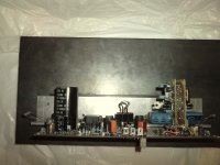
My own version of Alex PCB, ver 3.9 with the TO-3 final. As suggested by one builder, I cut the GND plane to isolate the different GND. I put a small insulated box over the front end active parts, and thermally coupled the transistors. I hope that it will reduce the DC offset drift cause by the front end thermal drift. That was one the original intent I guest of Goldmund module (in addition to hide the circuit...
The box is recycled from a GOES transmitter local oscillator enclosure. It is well shielded as well.
The PCB is of very good quality, heavy copper (I know it was difficult to grove), nice plating...
Still waiting for the TO3 mosfet, so I couldn't test it. I got a nice pair of huge 50Vac 500VA transformers.
I also order a nice enclosure with heatsinks, Goldmund style. I'll post my measurements.
Attachments
Last edited:
Very Very good job Algar_emi
The small insulated box it will reduce the DC offset drift.
Μy DC offset is +-/1mv at 55 C on mosfet case and 41 C on heatsink.SK57 300mm x 200mm.
BUT the the varies values of front end maybe give you a small DC offset drift.My new front end is stable 81V+-. I change on VAS 150Ω=180Ω 5,87 mA and the two resistors 330Ω to 390Ω ALSO 15KΩ=16.5ΚΩ with two resistors 33k and i have put 455Ω to give me 120mA per mosfet perfect balance on 3K resistors 3058-3058 mV.I reduce the input resistor 100KΩ to 22KΩ.
Also you must clip the four transistor on VAS face to face and all together.
Attachments
Last edited:


Hi, so was this the final one using these devices?Thanks guys , this time after many hours playng with my mouse , the job have done .I thing now it's quite good , if not I'm open to take critics from you .
Regards Alex .L.E. Error caps are 10.000 uF /100 vV not 63V like in the picture !
And how different is from the above one?
Thank you.
Last edited:
I can not decipher it, why on driver stage mpsa92 between collector and base has about 107V dc. Transistor mpsa 42 (U8), on base emiter have falling down voltage, and only this transistor is very hot, and i cant touch it, and its not inefficient. DC out is 38V. When measuring voltage from V- on bias resistor (R17, 270ohm) 107V, from other side 109V. Measuring from V+ on the same resistor 3.1V, and 5.1V. Any idea?
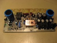
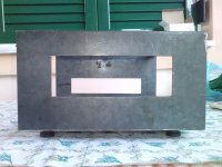
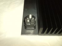
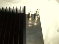
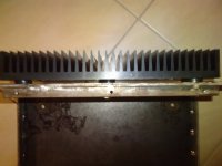
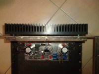
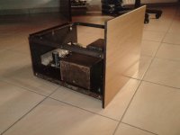
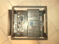
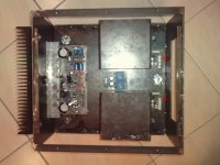
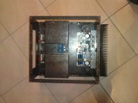
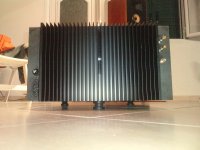
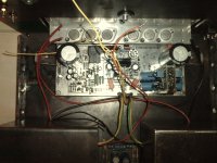
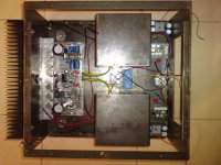
Goldmund 9.2
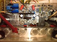
Goldmund 9.2 box.
Goldmund 9.2 box.
Attachments
-
 P140614_21.020001.JPG380.3 KB · Views: 268
 -
 P140614_21.030002.JPG287.5 KB · Views: 293
 -
 P140614_20.380003.JPG347.8 KB · Views: 262
 -
 P130414_21.240002.JPG475.2 KB · Views: 289
 -
 P140614_20.370001.JPG423.3 KB · Views: 212
 -
 P140614_12.540001.JPG506.1 KB · Views: 968
 -
 P020614_20.580003.JPG167.6 KB · Views: 1,011
 -
 P020614_20.580002.JPG153.1 KB · Views: 1,072
 -
 P020614_20.430001.JPG267.8 KB · Views: 1,121
 -
 P020614_20.410002.JPG293.7 KB · Views: 1,177
Member
Joined 2009
Paid Member
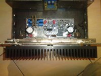
Amplifier looks good, but your bench is too tidy
I'm trying to do my best !!!
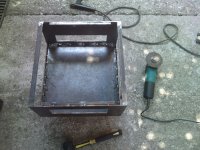
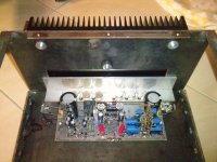
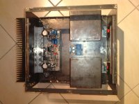
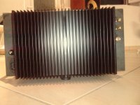
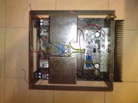
Re: Golmund clone
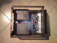
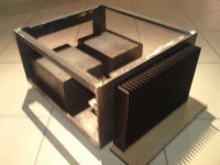
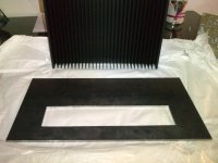
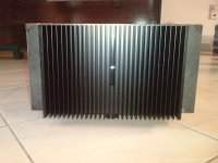
Golmund clone box
Golmund clone box
Attachments
Last edited:
- Home
- Amplifiers
- Solid State
- The Very Best Amplifier I Have Ever Heard!!!!