What type of separate regulated PS for VAS at +- 84VDC that you used?
Would you care to share the schematic so that we all could benefited from your findings.
Mikewong
Do you have construct the mimesis clone 9.2 ?
do you have problem because the main voltage 220v~ as input of the multiple capacitance varies up and down and result of this the offset goes up and down and the value of voltage on resistor R14 and R15 not equal .
can you show me your project?
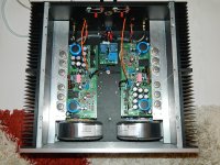
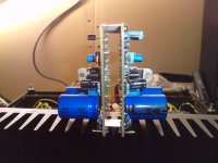
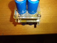
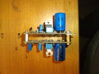
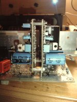
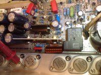
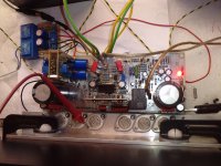
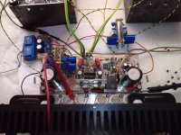
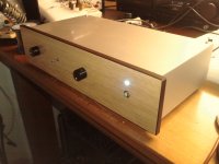
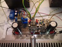
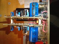
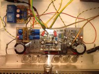
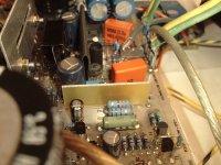
Now its time to put it on main board
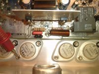
120ma per device 55-56 C on device 42C on heatsink as say it on manual.
Resistor R20 430Ω for 120ma +-/84v front end = 3035mv R14 3035mv R15 full load no fliker at all .
My friend Vit the drivers are KSA1381C KSC3503C
120ma per device 55-56 C on device 42C on heatsink as say it on manual.
Resistor R20 430Ω for 120ma +-/84v front end = 3035mv R14 3035mv R15 full load no fliker at all .
My friend Vit the drivers are KSA1381C KSC3503C
Attachments
-
 P130414_20.250001.JPG315.4 KB · Views: 958
 -
 P130414_20.560001.JPG303 KB · Views: 836
 -
 P130414_20.590002.JPG339.7 KB · Views: 785
 -
 P130414_21.000001.JPG429.7 KB · Views: 766
 -
 P130414_21.190001.JPG366.2 KB · Views: 249
 -
 P130414_21.270001.JPG259.7 KB · Views: 191
 -
 P130414_21.130001.JPG672.2 KB · Views: 249
 -
 P130414_21.320001.JPG549.4 KB · Views: 315
Last edited:
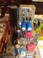
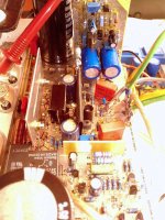
Now its time to put it on main board
120ma per device 55-56 C on device 42C on heatsink as say it on manual.
Resistor R20 430Ω for 120ma +-/84v front end = 3035mv R14 3035mv R15 full load no fliker at all .
My friend Vit the drivers are KSA1381C KSC3503C
Thank you very much!
Very spectacular your results
")
Best regards,
Vitali

I'm sorry to see that this is yet another thread that has become so diverse that it is pointless. As A DIYer it would be nice to be able to find a DIY design that could actually be copied at home. This seems to be a mixture of someone modifying some ancient old design vs a new PCB design that is full of flaws.
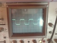
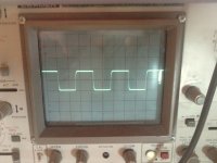
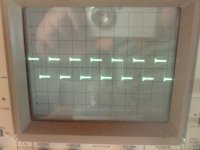
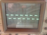
6) 100khz
7) 200khz
9) 1khz -1mf
5) 10khz-1mf
4) 20khz 1mf
7) 200khz
9) 1khz -1mf
5) 10khz-1mf
4) 20khz 1mf
Attachments
-
 P170414_16.490001.JPG263.5 KB · Views: 150
 -
 P170414_16.490002.JPG257.6 KB · Views: 138
 -
 P170414_16.580003.JPG286.8 KB · Views: 153
 -
 P170414_16.590003.JPG315.9 KB · Views: 177
 -
 P170414_17.300001.jpg502.7 KB · Views: 130
 -
 P170414_17.380001.JPG440.4 KB · Views: 119
 -
 P160414_21.580001.JPG471.6 KB · Views: 202
 -
 P170414_16.550002.JPG418.7 KB · Views: 151
 -
 P170414_16.590002.JPG277.7 KB · Views: 166
Last edited:
I'm sorry to see that this is yet another thread that has become so diverse that it is pointless. As A DIYer it would be nice to be able to find a DIY design that could actually be copied at home. This seems to be a mixture of someone modifying some ancient old design vs a new PCB design that is full of flaws.
I fully agree with you.
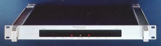
More than 20 years ago I fall in love with a mimesis 3, and loved to have mi own clone. Not only the circuit seems very good, the look of the slim amplifier was also important, so make a modified clone that only resembles the original (when looked from the distance)
Attachments
I'm sorry to see that this is yet another thread that has become so diverse that it is pointless. As A DIYer it would be nice to be able to find a DIY design that could actually be copied at home. This seems to be a mixture of someone modifying some ancient old design vs a new PCB design that is full of flaws.
I fully agree with you.
More than 20 years ago I fall in love with a mimesis 3, and loved to have mi own clone. Not only the circuit seems very good, the look of the slim amplifier was also important, so make a modified clone that only resembles the original (when looked from the distance)
It's time for you to show some new ideas and new pcb design.
I have a technical description of the mimesis 3 write by Martin colloms for hfn&rr more than 25 years ago.
Don't know if it infringes any copyright now, but if it is the case, Moderator please delete and sorry for the inconvenience.
very interesting reading, I recommend it to all on this forum
Don't know if it infringes any copyright now, but if it is the case, Moderator please delete and sorry for the inconvenience.
very interesting reading, I recommend it to all on this forum
Attachments

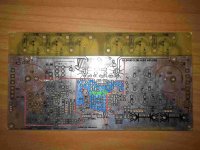
On reading this Thread, I still don't know what is the schematic of the mimesis 3, there are so many modified implementations.
just sure on one thing; it has only a pair of output mosfets...
there are some interesting topics on the article of hfn, and some inspiration for some.
when the thread started I still had the time and resources to try to implement a pcb, but not now, and still haven't the right schem...
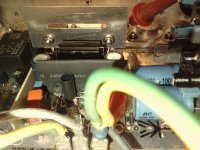
Τo all the friends who have built the amp this is the way to exterminate the offset :
+-/1-2 mV.
With a simple insulating between jfet and Vas plus insulating the jfet .
Isolating the input stage of the temperature coming out of the VAS and the nearby big resistor .
offset is always 1-2 mV and the value on resistors stable R1=3035mV and R2=3035mV.
120ma per device temp on heatsink 47C degree stable .
That's why the GOLMUND company enclosing the input stage to avoid the temp and for mechanical grounding reasons .The jfet transistor corroborate any defect.
Nikos
Attachments
Last edited:
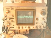
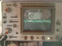
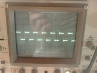
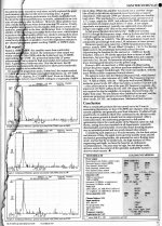
what is the timing of that repeating double spike? in pic 1 & 3
1ms
1khz
- Home
- Amplifiers
- Solid State
- The Very Best Amplifier I Have Ever Heard!!!!