Thanks EPCguy,
the diodes are a desperate measure. Somebody here remarked that 5V on the gate would kill the mosfets instantly, but OTOH the LM5113 wants at least 4.5V as Vdd. With Vdd=4.5V minus the diode drop, the mosfets would hopefully only go into a coma
Noted re the substrate connection.
I also found that the LM5113 already pulls down the two inputs (HI and LI) so the two resistors are not needed.
E
Elevator,
It is not as bad as all that . The abs max is 6V, but the gate leakage will start to increase beyond 5.5V. Initial 'discrete' driver boards were built with 5.6V supply and two 'matching' diodes - such that both low side and high side supplies are ~5V (EPC10XX devices required 5V for full enhancement).
EPC20XX devices are ok with 4.5V-5V and will even work at 4V for reasonable currents (plateau voltage not close to 4V). The LM5113 has an internal bootstrap diode and 5V on the supply will yield ~4.5V on the high side.
Adding a diode in series with the gate IMO makes a peak detector. With high Q this can lead to higher gate voltages (maybe?). The LM5113 pull up is 2Ohm internal and adding a series resistor will allow you to damp to the gate loop Q, such that 2Rgateloop>=Sqrt(Lgateloop/Ciss). This becomes harder for small devices and large gate loops (so keep the loop small and use wide/short traces). The gate resistance of the die is hard to measure, but ~0.6Ohm is a good WAG.
The Miller Ratio on these parts are worse than we'd like (i.e. >1), so a low impedance pull down is a must - especially the 100V/200V parts. This is why the LM5113 has a 0.5Ohm pull down. I'd suggest no series resistor for the pull down and again a short/wide trace as possible.
Hope this helps!..
Elevator,
It is not as bad as all that . [..] EPC20XX devices are ok with 4.5V-5V and will even work at 4V for reasonable currents (plateau voltage not close to 4V). The LM5113 has an internal bootstrap diode and 5V on the supply will yield ~4.5V on the high side.
Hope this helps!..
Good info, EPCguy. Seeing your nick, may we assume this comes straight from the horse's mouth?
Thanks in any case
E
PS re the substrate connection to source: I assume this is more a matter of bias rather than real working current?
Last edited:
Good info, EPCguy. Seeing your nick, may we assume this comes straight from the horse's mouth?
Thanks in any case
E
PS re the substrate connection to source: I assume this is more a matter of bias rather than real working current?
Hi Elevator,
Not sure why none of the emoticons are showing in my responses.

Yes, I'm a guy at EPC
")
The substrate current is much smaller than the device current, but can still peak at 1A, depending on dV/dt due to its capacitive coupling to the device. During 'hard' switching the Coss discharge/charge current can be as high as 15A.
Cool, welcomeHi Elevator,
Not sure why none of the emoticons are showing in my responses.
Yes, I'm a guy at EPC
The substrate current is much smaller than the device current, but can still peak at 1A, depending on dV/dt due to its capacitive coupling to the device. During 'hard' switching the Coss discharge/charge current can be as high as 15A.
Hi Elevator,
Yes, I'm a guy at EPC
welcome.
I have some questions for you, if you don't mind
In your demo boards (EPC9002), you only delay the turn on of the low fet , in the hi fet you use a Zero ohms resistor for R4, this is a typo ??
with a resistor of 2k and 10p for the capacitor the turn on delay is around 15ns, is this the recommended value or we can go lower?
what is the effective dead time, for the demo board?
The lm5113 uses a voltage clamp for the hi driver, because of the diode forward voltage drop of the low fet. but in your discrete solution you don't use none, do you have problems ?? or the conduction time of the low diode is to short to cause problems??
ok. now a tip
. The specifications of this fet are very good for class d use, but this type of package scares the potential users, I know you have to use this for minimize the parasitic inductance's, that can cause problems with the Vgs limitation , so the best solution is a driver integrated with the fets, do you have plans for this, if you do, can you speak a litle about your plans. sorry about the many questions
, and i have more... next timeCool.
No snubbers? Or gate resistors?
E
Hi Elevator.
It uses a gate pull-up resistance (0402) but not a sink resistance because of the problem EPCguy explain in the post #41 (preventing the Vgd charge to turn the low fet on wen the hi fet turns on).
This is not a final pcb, it just have the sensible parts on it, i am thinking on include the dead time control.
Sorry I didn't see the source (pull-up) resistors. Maybe you could post the schematics as well?Hi Elevator.
It uses a gate pull-up resistance (0402) but not a sink resistance
yeah, good thinking because dead time control is part of the tight timing environment.i am thinking on include the dead time control.
Unfortunately it takes pins, because you'd want to be able to set dead times from the outside: look at this
(attached)..
That's what we're doing here, DOH!...so the best solution is a driver integrated with the fets...
Attachments
Last edited:
In your demo boards (EPC9002), you only delay the turn on of the low fet , in the hi fet you use a Zero ohms resistor for R4, this is a typo ??
with a resistor of 2k and 10p for the capacitor the turn on delay is around 15ns, is this the recommended value or we can go lower?
what is the effective dead time, for the demo board?
The lm5113 uses a voltage clamp for the hi driver, because of the diode forward voltage drop of the low fet. but in your discrete solution you don't use none, do you have problems ?? or the conduction time of the low diode is to short to cause problems??
ok. now a tip
sorry about the many questions
Thx for the warm welcome.
I'll try to answer as much as I can.EPC9002 - the RCD pulse width adjust needs to adjust the required device deadtime as well as the mismatch in propagation delay (high side opto - no opto low side). It turns out I do not need to increase the HS pulse width - only delay and lengthen low side - therefore 'zero' on the HS adjust. Deadtime is relatively large for class-D (5-10ns)
and can be tuned smaller if it can be controlled over voltage / temp / pulse width.The values are conservative to make sure all boards don't have cross-conduction - probably could reduce it still a few more ns.
The discrete version has a single PWM input - since deadtime is controlled and minimized, the negative switch node voltage is too short duration to be an issue - those Si schottky diodes are pretty slow
. The board can be modified for two input operation, which will require an optional high side regulator (footprint for Mic5213) to avoid OV on HS with extended dead-time (such as isolated half-bridge application).There are many options for improving the 'usability' of our devices.
Wider pitch, better miller ratio, higher VTH and VGSmax, larger / better thermal package etc. Some are easier to do than others and are being looked into...
We are working with one or more companies to develop modules with our die and either controller / driver in a single package. All I can say - sorry.
On a personal note, I did spend a few years working on class-D and found it a unique field - like EMI/C - it is still a bit more art than science. Never had a good ear for it, but worked for someone who had a favorite sub-50Hz frequency and would talk about the 'color' or the music.

I mean a driver with a fet in a integrated circuit package, DOH!
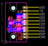
Very nice pcb, i like it very much elevator, congratulations, i think you are almost there.
Try to use thicker traces in the connection between the lt5113 and the fet.
wen i get free time i will send you a schematic of a dead time generator with only one variable resistor. maybe Monday. This weekend i will make some wine , not much time for electronic.
just discover this now:
http://epc-co.com/epc/documents/articles/EPC_Driving_eGaN_Transistors_fro_Maximum_Performance.pdf
Very nice pcb, i like it very much elevator, congratulations, i think you are almost there.
Try to use thicker traces in the connection between the lt5113 and the fet.
wen i get free time i will send you a schematic of a dead time generator with only one variable resistor. maybe Monday. This weekend i will make some wine
, not much time for electronic.just discover this now:
http://epc-co.com/epc/documents/articles/EPC_Driving_eGaN_Transistors_fro_Maximum_Performance.pdf
I mean a driver with a fet in a integrated circuit package, DOH!
This would be great - having a logic driven device / bridge. This is definitely a few years out and GaN has one big limitation here - no PMOS device (so not CMOS). Hard to make low Iq ICs this way.
Ha! I had jumped over 'integrated'. Apologies.I mean a driver with a fet in a integrated circuit package, DOH!
Very nice pcb, i like it very much elevator, congratulations, i think you are almost there.
Try to use thicker traces in the connection between the lt5113 and the fet.
wen i get free time i will send you a schematic of a dead time generator with only one variable resistor. maybe Monday. This weekend i will make some wine
just discover this now:
http://epc-co.com/epc/documents/articles/EPC_Driving_eGaN_Transistors_fro_Maximum_Performance.pdf
A one-resistor dead time generator would be excellent. Because the package looks already pin-limited now, and I don't want to sacrifice eg the temperature sensor, nor would I like a DIL arrangement instead of SIL like now.
OTOH I wonder if individual DT control for the high and low side would be needed / or could bring anything. I don't really think so though.
Happy winemaking! I just harvested about 15Kg only, sweet grapes but unsuitable for wine. Making grape juice and vinegarThis weekend i will make some wine
E
and GaN has one big limitation here - no PMOS device (so not CMOS). Hard to make low Iq ICs this way.
...and we're back to the days of RTL...
Thx for the warm welcome.
EPC9002 - the RCD pulse width adjust needs to adjust the required device deadtime as well as the mismatch in propagation delay (high side opto - no opto low side). It turns out I do not need to increase the HS pulse width - only delay and lengthen low side - therefore 'zero' on the HS adjust. Deadtime is relatively large for class-D (5-10ns)
The values are conservative to make sure all boards don't have cross-conduction - probably could reduce it still a few more ns.
The discrete version has a single PWM input - since deadtime is controlled and minimized, the negative switch node voltage is too short duration to be an issue - those Si schottky diodes are pretty slow
There are many options for improving the 'usability' of our devices.
Wider pitch, better miller ratio, higher VTH and VGSmax, larger / better thermal package etc. Some are easier to do than others and are being looked into...
We are working with one or more companies to develop modules with our die and either controller / driver in a single package. All I can say - sorry.
On a personal note, I did spend a few years working on class-D and found it a unique field - like EMI/C - it is still a bit more art than science. Never had a good ear for it, but worked for someone who had a favorite sub-50Hz frequency and would talk about the 'color' or the music.
Yes, i see now, you only use the optocoupler for the high side.
If you use the two optocouplers (no mismatch in propagation delay), what will be the value of the resistence in the RCD circuit?
5ns-10ns of dead time is not a problem, there are ways of dealing with that.
One way is making the output inductor current ripple larger than the load current. As long as the inductor current ripple is larger than the load current at the moment of switching, its current is in the right direction to force the switch node voltage to begin slewing to the other rail immediately in the beginning of dead time. So no dead time error. this method is not widely use because of the relative high Rds of the output mosfet (increase conduction loss), but this is not a problem with the eGaN FET as they have very low Rds resistance. I use another method .
"those Si schottky diodes are pretty slow
."Are you referring to the BAV19WS? they are not schottky.
I am thinking in using a lm317 instead of the lt3011 for the 5.6V, is any problem with that?
And, if i go with a discrete solution (probably i will). I will use the Complementary mosfet BSD235c instead of the Sia513,it has a Qg of only 0.4nc and Rds 350mohm (N Channel) 1200mohm (P Channel). I think it is a better choice, as the Sia513 is no longer recommended for new designs, by Vishay ,and need a higher gate charge.
Also, Tacky flux (Kester TSF-6592LV) with no solder paste or stencil works well. Be sure that all flux is cured before before applying power to avoid dendrite (tin whisker) growth.
Thanks for the tip .
The RCD circuit will then just be the deadtime +/- the matching error between the two paths. Could be around 100 ohms or so.Yes, i see now, you only use the optocoupler for the high side.
If you use the two optocouplers (no mismatch in propagation delay), what will be the value of the resistence in the RCD circuit?
5ns-10ns of dead time is not a problem, there are ways of dealing with that.
One way is making the output inductor current ripple larger than the load current. As long as the inductor current ripple is larger than the load current at the moment of switching, its current is in the right direction to force the switch node voltage to begin slewing to the other rail immediately in the beginning of dead time. So no dead time error. this method is not widely use because of the relative high Rds of the output mosfet (increase conduction loss), but this is not a problem with the eGaN FET as they have very low Rds resistance. I use another method .
Doh. Yes the EPC9001 uses schottkys. The EPC9002/3 are the BAV19/21"those Si schottky diodes are pretty slow
Are you referring to the BAV19WS? they are not schottky.
I am thinking in using a lm317 instead of the lt3011 for the 5.6V, is any problem with that?
And, if i go with a discrete solution (probably i will). I will use the Complementary mosfet BSD235c instead of the Sia513,it has a Qg of only 0.4nc and Rds 350mohm (N Channel) 1200mohm (P Channel). I think it is a better choice, as the Sia513 is no longer recommended for new designs, by Vishay ,and need a higher gate charge.
The reason for the LT was a small regulator with a PGOOD - this acts as UVLO to have both fets off when the bias supply is removed (else "BANG"). If sequencing is ok, then any old regulator should do. I find the LT3011 being limited to 50mA is limiting for HF on the EPC9001 for going past ~2MHz.
I agree - I've tried to replace the SiA513 with the 511/519, but they have too large a gate change and too slow if you still want the pre-drive to realize the offset voltage to avoid cross conduction in the final stage. Still looking for a replacement. Si1563? (haven't got around to trying it yet)
The BSD235c seems a good choice although I'd like to see it in the thermally enhanced DFN package. You may have to also adjust R9, R10 for best speed / zero cross conduction.
man this is turning out to be very nice... now you will start to look that some big company (in china or something like that) won't copy this and sell it
There is no reason to think that they could not.
I am convinced: They could.
Likely - it is more a commercial question, when GaN for turns attractive for class D amps from financial perspective.
...And that's one reason why we are keeping quiet lately.There is no reason to think that they could not.
E
- Status
- This old topic is closed. If you want to reopen this topic, contact a moderator using the "Report Post" button.
- Home
- Amplifiers
- Class D
- The Uber eGaN Half-Bridge Module