I have been playing with your cap multiplier some days ago. Increasing the filtering at this stage seems not usefull, even if we reduce the ripple on filtered power supply, the ouptut doesn't reduce any more, other path is expected (directly to OPS).
Anyway, the results I had were not as stellar. Will check that one day.
Anyway, the results I had were not as stellar. Will check that one day.
I'm just learning here, so please take this as a newbie question, not as a criticism !
I've been thinking about power and ground distribution, and in particular about the capacitance multiplier. One point Cordell makes in his book is that this circuit allows you to take the reference with respect to the quiet ground (IS + VAS), while allowing ground current from the filter capacitor (C8 in previous schematic) to flow through the more noisy ground (OS). I don't have the book with me, but I recall that he actually uses two different ground symbols in his example schematic.
I understand (and appreciate) the advantage of dividing the Mongrel design into separate amp/power modules, but it seems like a capacitance multiplier sort of straddles the boundary. From a noise (PSRR) point of view, wouldn't it be better to put R23/C8 on the power board, and the rest on the amp board ? Then the AC ripple current flowing from the power rail through C8 to ground would be kept local to the power board, and the (much more highly filtered) voltage on C10 referenced to a (presumably much more quiet) ground on the amp board would result in a cleaner output voltage.
Again, I don't expect you to change designs at this stage; I'm mainly wondering if the idea makes any sense.
I'm just learning here, so please take this as a newbie question, not as a criticism !
I've been thinking about power and ground distribution, and in particular about the capacitance multiplier. One point Cordell makes in his book is that this circuit allows you to take the reference with respect to the quiet ground (IS + VAS), while allowing ground current from the filter capacitor (C8 in previous schematic) to flow through the more noisy ground (OS). I don't have the book with me, but I recall that he actually uses two different ground symbols in his example schematic.
I understand (and appreciate) the advantage of dividing the Mongrel design into separate amp/power modules, but it seems like a capacitance multiplier sort of straddles the boundary. From a noise (PSRR) point of view, wouldn't it be better to put R23/C8 on the power board, and the rest on the amp board ? Then the AC ripple current flowing from the power rail through C8 to ground would be kept local to the power board, and the (much more highly filtered) voltage on C10 referenced to a (presumably much more quiet) ground on the amp board would result in a cleaner output voltage.
Again, I don't expect you to change designs at this stage; I'm mainly wondering if the idea makes any sense.
On the power boards ,C8/10 ARE referenced to a fully separate ground (G2). The 2 cap multipliers can even be run from a totally separate PS (Vcc2/Vee2). Any way you might want to do it ... many options ! What you saw was just the simulation , the real boards are "split" different.
OS
Yeah , just models ....
Real life is different , I have used my new CRO probes extensively (just pokin' around) and the actual performance is slightly short of what the simulation predicts. Voltages are right on , currents are right on , but ground and rail ripple are much more dynamic with an actual signal. The single device multiplier with a second order setup is good to about 1V main rail ripple. This can be improved by sacrificing more rail voltage with the multiplier resistive divider. With a darlington multiplier you still have to sacrifice 2-3V , but the ripple drops way below 1mV.
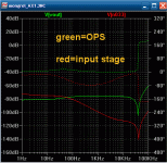
(below) is what the normal 1st order R/C input stage filtering will get you , PSRR wise. No filtering at all plots out 3dB worse. This must be the amp's "natural" PSRR (-80db). I will say it ... this is ALL you will get building most of the amps on this forum. You can go dual mono , but still have each individual channels ripple to contend with...Good old PS IM at 200w+ output. None of this matters much at normal listening levels , as PSRR scales with output.
OS
Real life is different , I have used my new CRO probes extensively (just pokin' around) and the actual performance is slightly short of what the simulation predicts. Voltages are right on , currents are right on , but ground and rail ripple are much more dynamic with an actual signal. The single device multiplier with a second order setup is good to about 1V main rail ripple. This can be improved by sacrificing more rail voltage with the multiplier resistive divider. With a darlington multiplier you still have to sacrifice 2-3V , but the ripple drops way below 1mV.
(below) is what the normal 1st order R/C input stage filtering will get you , PSRR wise. No filtering at all plots out 3dB worse. This must be the amp's "natural" PSRR (-80db). I will say it ...
this is ALL you will get building most of the amps on this forum. You can go dual mono , but still have each individual channels ripple to contend with...Good old PS IM at 200w+ output. None of this matters much at normal listening levels , as PSRR scales with output.OS
Attachments
you will find many ClassAB Power amps that "hum" more when the bias is turned up........... None of this matters much at normal listening levels , as PSRR scales with output.
By the time the bias is upto optimal ClassAB bias the "hum" can be quite strong.
This is obviously a fault in the amplifier, but what it shows is that quiescent current has an effect on the Quiescent PSU ripple voltage and this ripple voltage can leak into the amplifier circuits. It does not scale with power output.
It's exactly the opposite, it is more annoying at low to zero watts of output power.
Underpowered ?? or just 1 pair rail caps ? (ESR) Is that why some like 10 pair of smaller caps in parallel ? My 8- 8.2K's do better (ripple wise) on the CRO than my 4 -4.7K's do with my smaller mongrel. My big amp has been biased to over 200ma/device , but still no hum. Must be that 65K doing it's job. ")
PS , what I did on the sim was just to reduce the artificial ripple from 1 V to .25v.
OS
PS , what I did on the sim was just to reduce the artificial ripple from 1 V to .25v.
OS
On the power boards ,C8/10 ARE referenced to a fully separate ground (G2). The 2 cap multipliers can even be run from a totally separate PS (Vcc2/Vee2). Any way you might want to do it ... many options ! What you saw was just the simulation , the real boards are "split" different.
OS
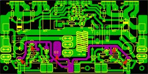
Well, if I look at the layout for PB120N, the ripple/noise current flowing through C91 (100 uF filter cap) flows through the G1 trace that serves as the ground reference for C91 (the "multiplied" cap") and the voltage divider, and then continues some distance to the G2 terminal where it flows through a "long' wire before it gets back to the HQG point. So the ripple current through C91 is contributing to the amplitude of the cap multiplier output. My interpretation of Cordell's description is that C91 should connect not to G1 but to the noisier G2 trace.
Well, if I look at the layout for PB120N, the ripple/noise current flowing through C91 (100 uF filter cap) flows through the G1 trace that serves as the ground reference for C91 (the "multiplied" cap") and the voltage divider, and then continues some distance to the G2 terminal where it flows through a "long' wire before it gets back to the HQG point. So the ripple current through C91 is contributing to the amplitude of the cap multiplier output. My interpretation of Cordell's description is that C91 should connect not to G1 but to the noisier G2 trace.
I see your point now. In theory you are right, but have the "G's" reversed (Below).. G1 = noisy - zoble / OPS decouplers - G2= clean -VAS/IPS. The initial "dirty rail pulses" from the main PS go through R79/83 to the first decoupling caps (C87/91) , I agree ... with a single supply , these caps should go to G1 (dirty ground). On the real amp (I have 4) , the actual ripple and the ground pulses measured at G2-C87/91 are 1mV or below. Since the voltage stages use only +/- 18-25ma , very minimal switching pulses are present at the first 2 caps (R79-83 are "lift" resistors). So , seeing that I had sub mV ripple at C91 and might have a dual power supply (second set of fastons V+ / V-) ... I chose to make G2 the common star for BOTH sets of caps associated with the multiplier.
The end result of this is that I have my desired .1mV ripple at the 2 Voltage stage rails (at a -2V penalty) and scoping G2 , the ripple is nearly immeasurable at full output of the amp. I have a "non-multipliered" CDRC (cap/ diode/ resistor/cap) power board (the PB60X2) , this is my 60W test amp and pretty much the standard fare here at DIYA. It has the standard single ground star configuration. I can see .1-.25 VOLTS !!! on the voltage stage rails and the ground ripple is measurable. For the PB120/250 , I had to come to a minor compromise which did not degrade performance but allowed for the optional second voltage amp power supply option. I DID think this out (reckoned it
) in every way before I finalized the design. The only benefit to the G1/G2 setup is with a "split" power supply board (PS100) ... 2 banks of capacitors with the appropriate "lift resistor" between banks. The voltage boards also have a "lift" resistor/double diode (D1-2/R3) for the CCS/ input stage.OS
Attachments
You got it. (1A - 1n4001 or equivalent)I am still unclear about D1 and D2 shunting R3.
Are the diode ratings useful for ground fault current duty or do they serve some other purpose ?
OS
For offset trimmer on AX board(R13) could a 2k trimmer be used without to much trouble?
Even a 5K , you would change the unity gain point downwards by 50K with more phase margin. If you went the other way (500R) UG would increase but still be way within safety margins. If you are using the present AX layout , change R22 to 10k and tie it to C5. The new AX PCB update (post 1301) has this change , no cascode and Cordell's safety device on the VAS. The improvement in turnon is dramatic , going from a "tick" (not quite a thump) to NOTHING.
In the final package , I will expand the 1301 board to cascoded/non-cascoded versions , plus... for the cascoded version ,make that one universal for BCxxx or MPSA IPS devices.OS
Thank you OS.
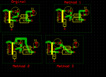
R22 is now changed to 10k. But im really not sure how to tie it to C5..
Could you take a look at the attached picture and tell me wich method is correct?
Ohh, another thing, i just found out ive forgot to order 390pf - C2 on AX board, could i use 330pf or 470pf? Those i do have, haha
EDIT: i also have 2pcs 180pf, 2 in parallel would give 360pf...
Attachments
Last edited:
Thank you OS.
R22 is now changed to 10k. But im really not sure how to tie it to C5..
Could you take a look at the attached picture and tell me wich method is correct?
Codegen :
I just read back a little and post #1290 has a schematic and some explanation.
Thank you OS.
R22 is now changed to 10k. But im really not sure how to tie it to C5..
Could you take a look at the attached picture and tell me wich method is correct?
Ohh, another thing, i just found out ive forgot to order 390pf - C2 on AX board, could i use 330pf or 470pf? Those I do have, haha
EDIT: i also have 2pcs 180pf, 2 in parallel would give 360pf...
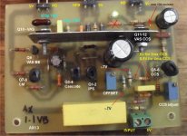
330p will just raise the input HP filter a little , 470p will lower it. Neither will be anywhere close to the audio band. As far as the 10k resistor ... look below (pix) , drill 1 hole .. all done !
OS
Attachments
So what do you (OS) or others feel about speaker protection with the Mongrel ?
I'm confident in my soldering and assembly abilities, but I have no way of knowing what the risk is of a catastrophic, speaker-killing failure is. Is there anything about this design that makes it less likely ? Do failures occur mainly due to "predictable" things like under-rated parts, over-use (hours, temperature), power line garbage, turn-on stresses, or do transistors just sort of up and die ?
In my case, I wouldn't mind too much if some of my silicon smoked, but I'd be very unhappy if I had to shell out for a new set of drivers. I kind of want to avoid speaker relays, but I'm toying with the idea of adding a triac to shunt output to ground if case of excessive DC.
Are there any plans in the works to make speaker protection part of the design ?
330p will just raise the input HP filter a little , 470p will lower it. Neither will be anywhere close to the audio band. As far as the 10k resistor ... look below (pix) , drill 1 hole .. all done !
OS
Ahh, okay, now i see. Thank you!
Maybe there will be sound to hear from it tomorrow :=)
- Status
- This old topic is closed. If you want to reopen this topic, contact a moderator using the "Report Post" button.
- Home
- Amplifiers
- Solid State
- The MONGREL (supersym II)