There are very few things more laborious than getting that part the right size and of sufficient quality, simultaneously. Eventually, the results can be very beautiful, but I'm just saying that availability doesn't actually mean easy.but maybe not for every application, especially nowadays with good capacitors available at reasonable cost for the role of DC blocker in the FB loop of a non-inverting chipamp.
no doubt about it, the inverting topology is much easier.
but it still needs authentic chips -- laser engraved lettering, extremely smooth backside.
have you tried a nichicon muse np or similar for the non-inverting dc block?
(see non-inverting bom a bit above the earth grounding pic.)
but it still needs authentic chips -- laser engraved lettering, extremely smooth backside.
have you tried a nichicon muse np or similar for the non-inverting dc block?
(see non-inverting bom a bit above the earth grounding pic.)
Last edited:
BTW, about pins: i don't break off any 7293 pins even if the build initially won't use all pins. the reason is that the 7293 has no NC pins. every pin connects to something. i don't want to box myself in by removing a pin that i don't need right now, because "later" has this very annoying habit of turning out different from "right now".
Are these (attached) the currently preferred component values for TDA7293 Inverting T-Net?
Has it been auditioned yet?
HI
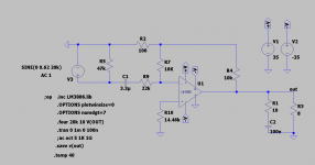
on symulation with LM3886 I found 0.3% distortion at 50W 8ohm, and 0,05% with simple inverting mode with 20K / 1k or 200K / 10K with
Last edited:
that's a surprisingly large difference.
in the sim did you have a series R and a shunt R in the non-inverting amp's + input (to give it a 0v reference)?
to me the non-inverting amps (3886 and 7293) sound pretty good but i have the input circuits and FB wired very compact point-to-point and use ELNA caps for the DC block cap between the FB shunt R and audio ground (which is lifted by 1r5).
Last edited:
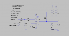
a couple of possible sources of error terms:Here are the diagrams
in the sim's t-net schematic, one end of R2 ties to SigIn ground. but in the real circuits R2 ties to a ground star that includes the PSU 0v and the load return.
in the real circuit, R10 ties to the SigIn ground and the SigIn ground is lifted by 1R5 to the PSU/speaker/R2 ground star. The power pin bypasses also tie to this star, which isn't shown at all in the sim.
Last edited:
@sfthurber
I certainly would like to see your recommended non-inverting t-network TDA7293 schematic, without a tube, without a buffer, without a preamp.
And, I would also like to see your recommended Inverting t-network TDA7293 schematic, without a tube, but it is okay to assume preamp/buffer for constant input impedance.
well, i wouldn't use any inverting topology without a buffer (at least) in front of the inverting stage, because without the buffer the preceding stage (and any interconnects between the previous stage and the inverting stage) will become part of the NFB loop for the inverting stage. not good.
the first schematic it the first post's schematic link is fine.
all the grounds in it are audio ground.
use a 1r5 from there to the power star gound (which is also the load return).
i should add that i need to update the first post to reflect what i've done lately with 7293.
since i found almost no difference inverting vs non-inverting i've gone back to using the Fly-xy version of your favorite board but buildin the NFB and input circuit point-to-point on the underside of the board with 1k/30k in a conventional NFB loop (not a t-net).
non-inverting has the advantage that the mute circuitry works while inverting breaks the mute function for reasons that are obvious if you look at the datasheet.
Last edited:
forgot to mention, the non-inverting circuit that i actually use ends up like the next-to-last one in the linked-to drawing. it's a non-inverting chipamp driven by a differential (XLR) input tube stage. v4 and v6 are a noise and balance selected 6922 dual triode (so one envelope per channel), c2 is the 400v poly, c14 is the Elna cap. all the shown grounds are the SigIn ground star. one could optionally chose to replace the anode resistors with a current mirror.
Last edited:
not sure what your questions might be at this point.
to recap--
as discussed in the first post:
the that post (in the third paragraph after the preface) there is a link to a schemas document. the first schematic in the document (top left) is the simplest one for the inverting power amp stage.
the second row of schemas in the document, at the left, is a unity gain buffer.
we've discussed power amp passive parts values already and they are reflected also in the BOM. the buffer parts are also in the BOM just below the parts list for the power amp.
decibel dungeon also has some helpful buffer discussion as do posts by carlosfm.
what specifically remains a mystery to you at this point?
i'll be glad to answer specific questions.
- Status
- This old topic is closed. If you want to reopen this topic, contact a moderator using the "Report Post" button.
- Home
- Amplifiers
- Chip Amps
- TDA7293 inverting t-network FB point-to-point