MOSSEN
Green output: MOSS
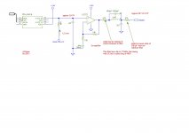
This is the output I have in mind (1543 Vdd 7V) and the comparison to the standard SEN (with 1543 Vdd 5-6V).
This MOSS I have used before with a triode as cascode. Extremely linear and no overshoot at all. With a triode the Vb becomes some 120-150V.
View attachment SEN+MOS-SEN.pdf
Green output: MOSS
This is the output I have in mind (1543 Vdd 7V) and the comparison to the standard SEN (with 1543 Vdd 5-6V).
This MOSS I have used before with a triode as cascode. Extremely linear and no overshoot at all. With a triode the Vb becomes some 120-150V.
I used it on TDA1541 and when I 'shorted' the output with an extra 50 ohms there was no effect on the output RMS, so the input impedance is very low.
View attachment SEN+MOS-SEN.pdf
Pin 7 is left floating and +3v from a couple of 1.5v batteries is fed to the other two resistors (Pins 6 & 8).
I think I did roughly the same thing when I created a voltage divider from +5V to ground, loading pins 6 and separately pin 8 (left and right channels). The Thevenian equivalent circuit looking like 2 to 3V (depends on the resistors selected) and around 1.3K or so, as an I/V conversion circuit.
An externally hosted image should be here but it was not working when we last tested it.

FFSS
Remember the logo ffss on some of the first vinyl discs?
Full Frequency Stereo Sound.
Well, that is the effect I have now with my latest version of the TDA1543 in a single solution.
Thanks to fliedegg I started to float pin 7, this implies there is no 'extra' current dumped by pins 6,8 and thus the output must float at around the same voltage; ECdesigns uses 3 - 3,2 Volt from lead batteries.
Leaving the pin floating is indeed a large improvement, the coarseness that is often heard in the TDA1543 is completely gone.
Next improvement I found is that it is best for the high frequencies to buffer the output from the pins 6, 8 before going to the filter.
I have used a TLC272 opamp, a curious device as it was made for single supply use. I use the same 7 volt as the Vb for the opamp.
This is the marvelous result of the combined filters effect:

As you see the whole staircase (stepwise response) is filtered out in a superb way. 4fOS, the main filter has the dip at 175 kHz. I use the opamp in a 2x amplification.
I have played around with the bias voltage; I started at 3,8 V and it can be increased to 4,1 v (which is best to center the output between the voltage rails). The Pin 6, 8 output floats along with this bias (the current source has a 380 kOhm virtual impedance) from 2,9 - 3,2 V DC.
The sound: FFSS of course, and a very tight bass (better than with my TDA1541 S2/SEN) while the highs are sibilant and the crescendo and forte passages have no problem at all. The output cap is critical in this aspect I noticed. It is a pleasure to listen to.
Not as warm (tubey) yet as I would like but not cold at all.
Turning the volume knob all the way - shows no background noise.
So my breadboard is successful up till now.
Remember the logo ffss on some of the first vinyl discs?
Full Frequency Stereo Sound.
Well, that is the effect I have now with my latest version of the TDA1543 in a single solution.
Thanks to fliedegg I started to float pin 7, this implies there is no 'extra' current dumped by pins 6,8 and thus the output must float at around the same voltage; ECdesigns uses 3 - 3,2 Volt from lead batteries.
ECDesigns bias tweak can be found here.
http://www.diyaudio.com/forums/digi...-tda1541a-286.html?postid=1813308#post1813308
Pin 7 is left floating and +3v from a couple of 1.5v batteries is fed to the other two resistors (Pins 6 & 8).
Leaving the pin floating is indeed a large improvement, the coarseness that is often heard in the TDA1543 is completely gone.
Next improvement I found is that it is best for the high frequencies to buffer the output from the pins 6, 8 before going to the filter.
- With the filter directly connected to the pins I have noticed the high frequencies are reduced a bit. The sound is very "TDA1541-like", which is not bad by the way.
- With a buffer in place the high frequencies are all there
I have used a TLC272 opamp, a curious device as it was made for single supply use. I use the same 7 volt as the Vb for the opamp.
This is the marvelous result of the combined filters effect:

As you see the whole staircase (stepwise response) is filtered out in a superb way. 4fOS, the main filter has the dip at 175 kHz. I use the opamp in a 2x amplification.
I have played around with the bias voltage; I started at 3,8 V and it can be increased to 4,1 v (which is best to center the output between the voltage rails). The Pin 6, 8 output floats along with this bias (the current source has a 380 kOhm virtual impedance) from 2,9 - 3,2 V DC.
The sound: FFSS of course, and a very tight bass (better than with my TDA1541 S2/SEN) while the highs are sibilant and the crescendo and forte passages have no problem at all. The output cap is critical in this aspect I noticed. It is a pleasure to listen to.
Not as warm (tubey) yet as I would like but not cold at all.
Turning the volume knob all the way - shows no background noise.
So my breadboard is successful up till now.
Not as warm (tubey) yet as I would like but not cold at all.
I'm not sure that this helps but get my Tda1543's I2S via a CS8412 and after going back through the archives I found that grounding was very important to the final sound.
I therefore have two set ups - one with the analogue and digital grounds merged early on for the nice tubey warmth that helps my electronic music cd's.
The other has the A/D grounds kept separate until a star ground is applied. This gives a nice cold/harsh but alive feel for my 70's rock cd's.
My point is that the final sound is (of course) also affected by matters upstream of the DAC.
I'm not sure that this helps but get my Tda1543's I2S via a CS8412 and after going back through the archives I found that grounding was very important to the final sound.
I therefore have two set ups - one with the analogue and digital grounds merged early on for the nice tubey warmth that helps my electronic music cd's.
My point is that the final sound is (of course) also affected by matters upstream of the DAC.
I found a document on grounding where the idea was to connect as early as possible, the main reason stated for difference between A and D grounds is that the substrate of the chip requests such. In the TDA1543 there is already one pin only. So in effect it has combined A&D.
Assume this is the cdtubed. Just pondering. Might the long distance to the star ground have inductance on the chip? Would decoupling locally have any effect?The other has the A/D grounds kept separate until a star ground is applied. This gives a nice cold/harsh but alive feel for my 70's rock cd's.
Attachments
I found a document on grounding where the idea was to connect as early as possible, the main reason stated for difference between A and D grounds is that the substrate of the chip requests such. In the TDA1543 there is already one pin only. So in effect it has combined A&D.
Having had a bropwse around I think this is a peculiarity with the CS8412 and not a general thing.
The chip is rather old so I can't find more info but this site refers to the effect at the bottom of the page.
Input Receiver
> sen can't have any dc offset on it's input.
Of course it can.
Else how would all these ES9018 builds function perfectly.
And those who insist on wiring SEN to a fixed (instead of floating) supply, or using the same supply for both channels, simply do not understand how the circuit works. They are much better off using the cascoded CEN from Loesch.
http://www.diyaudio.com/forums/digi...minimalistic-iv-converter-31.html#post3655847
Patrick
triode Al could You post last diagram of output stage you used?
tx
(it is not quite clear tome what You did on the L/R ots pins and Vref pin)
Here is my last incarnation. Floating pin 7 sounds best. Great thanks!

I have some further thoughts on the output. Room for further investigation.
As for nowe, I am pretty happy.
I tried the filter (sans the 470 ohms) directly on the output, but this has influence on the highs (not a bad one though).
The filter tested with 510 ohms (35 ohms generator + 470 input) gives - 1dB at 20 kHz; this is only achieved with the 2,7 nF at the output. With 2n7 there, the bridging cap is sensitive and determines the dip (notch); I tested experimentally and found 940-960 was giving me the nulling at exactly 176 kHz.
Here's a first stab - its assuming the 1mHs have no frequency dependent losses - a major assumption. The working impedance is 100R, set by the desired corner freq and your inductors.
Having the filter after the buffer I can now easily test this design
Thanks
I didnt try yet with N.C. Vref pin but I will
Vhat is the voltage on floating Vref pin?
Did You measure maybe?
.
I made some dac before 5-7 years with 16 tda1543 in parallel
And I can say that temperature is from the vital importance.
Keeping the temperature as much is essential.
as NON inductive Riv
(You can use maybe SMD one I think that they are not induvctive like MF?)
or 10x carbon in parallel to match desired value.
.
It is much better to have a reactive network after the driver-buffer.
than on the direct output on the dac chip.
.
this dac is very very good, brings some live component to the music.
I like this chip.
.
now for the output of some sh...t sound card I am using
Zanden style multiplyed notches networks for Fs=44.K
Fs, sqtr(Fs x 2Fs), 2Fs
.
Irrespective of the load and voltage on pin 6, 8 the vRef "supplies" about 2,18 volt (in practice there is a slight drift, initial 2,202 and 2,173 after 10 minutes). Probably thermal in nature.Thanks
I didnt try yet with N.C. Vref pin but I will
Vhat is the voltage on floating Vref pin?
This floating pin 7 is also the standard structure of the data sheet (where the vRef is used for the bias of the opamp)
Output pins now dump 1,2 mA instead of supplying it like when a resistance is connected to earth. That is why my bias is higher than the output DC. With floating pin 7 I did not get output unless there is a floating bias.
What does that look like? I understand it is only for NOS?Zanden-style multiplyed notches networks for Fs=44.K
Fs, sqtr(Fs x 2Fs), 2Fs
.
"This floating pin 7 is also the standard structure of the data sheet (where the vRef is used for the bias of the opamp)"
exactly
(Yes thermal nature)
I recommend little heat-sink even for the one chip used...
.
not only for the NOS i think?
in original idea it is 5 or more nets starting with the desired Fs and n x Fs (n=1..5 or more) I used just 2 stages and one in between because it is after the interstage trafo.
(I used ferrite beads for L element, which is NOT proper and not good, but I want to sniff it a bit...). Zanden concept idea You can find on the net in form of patent papers
.
I spot that the Voltage have phase shift after the any simple Riv conversion.
So maybe the OP amp You used should be in inverting mode of operation,
to achieve more correct phase on the output...
dont take me wrong, like criticizing Your work - it is not,
that is simple suggestion to check

I spot that the Voltage have phase shift after the any simple Riv conversion.
So maybe the OP amp You used should be in inverting mode of operation,
to achieve more correct phase on the output...
dont take me wrong, like criticizing Your work - it is not,
that is simple suggestion to check
.
I spot that the Voltage have phase shift after the any simple Riv conversion.
So maybe the OP amp You used should be in inverting mode of operation,
to achieve more correct phase on the output...

I think you are right; but I had trouble in adjusting the gain because the bias is also amplified so I went for the quick and dirty non-inv solution.
Yes i think that is Vref pin is just for some ”thermal dynamic” voltage reference source
(not current)
not to supply something (like Vref resistor or so...)
it is not un-logical, when it is not in use to disconnect it...
what do You think?
Any current from pin 7 is reflected on the output pins probably with some kind of current mirror; that is the trick that is used to have a resistor to ground with higher Vb. So having any resistor in place with a different structure might be strange.
However, thinking about it:
- the output now takes in 1,2 mA; what would happen if the load on the Vref changes that current demand to an equilibrium, such as 0,0 mA versus a given bias?
I dont know really what would happened in that case?
maybe it is not possible because of the spacitances current leakage,
You said that it is a part of the current mirror?)
(not sure, because I am not an expert...)
.
maybe this Vref pin should be somehow isolated
with an external circuit like voltage reference
and then used next in a IV device or so for biasing etc...
.
second what would be happened if we put some AC filter on it
or little capacitance.
.
Is it some AC signal on Vref pin when dac is in the opperation?
The Vref pin has two functions:
- setting a voltage reference for the external I/V (Vref pin is an output)
- adding an offset current to the output (Vref pin is an input)
The typical opamp virtual ground I/V circuit, as shown in datasheets, uses the first Vref function.
The typical grounded resistor passive I/V, as used in many NOS circuits, usually uses the second function.
- Status
- This old topic is closed. If you want to reopen this topic, contact a moderator using the "Report Post" button.
- Home
- Source & Line
- Digital Source
- TDA1543 semi-parallel solution