Hi, Mr.Evil,
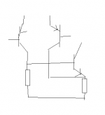
I dont understand the position of the FC's reference resistors (R1-R2-R3-R4) are refered to output? What effect is happening with this configuration? To lower the OL gain? Shouldn't it is better to have those R's put to steady ground to have steady FC work?So I tried the same on mine - replacing the bias voltage for the cascode stage with a simple resistive divider and feeding back the output to the centre of it.
The problem with fully differential topology is that because there is no reference to ground, it is impossible to be certain of the output voltage relative to ground. What happens in practice is that although the quiescent DC voltage between the outputs is zero, the outputs will both be hard up against one of the supply rails.
Differential-mode feedback cannot fix this, so common-mode feedback must be applied. This is the purpose of connecting the cascode bias dividers (R1-4) to the output. This tends to pull the outputs towards the centre of the two supply rails, which is ground. The fact that it reduces open loop gain is just a side-effect.
Differential-mode feedback cannot fix this, so common-mode feedback must be applied. This is the purpose of connecting the cascode bias dividers (R1-4) to the output. This tends to pull the outputs towards the centre of the two supply rails, which is ground. The fact that it reduces open loop gain is just a side-effect.
Ah, I see now. In the v3proto.pdf, the ground reference by R1 and R2 is not good enough?
Dispite of its good purpose, like you said, putting the FC's reference to output will add THD, because the base of the FC's are modulated, while if we put R1-4 to ground the bases will be steady, wouldnt it?
Dispite of its good purpose, like you said, putting the FC's reference to output will add THD, because the base of the FC's are modulated, while if we put R1-4 to ground the bases will be steady, wouldnt it?
Although it looks like R1 and R2 should help, it's not possible to affect the common mode DC offset in that way since they feed into the differential input, and any input there affects both sides equally. I think the purpose of those two resistors is to help stop the inputs floating, which could cause a nasty pop if an input is connected while the amp is powered on.
Feedback to the reference does increase THD, but it also decreases THD by providing local feedback around the output stage. Overall the effect is quite small.
Feedback to the reference does increase THD, but it also decreases THD by providing local feedback around the output stage. Overall the effect is quite small.
Thanh: Personally I would consider this to be a variant of a normal VAS.
It is true that by varying the resistor values, you can achieve operation closer to normal VAS, or to FC. However, "closer to" and "being there" are not the same things.
When I design an FC, I am looking for things like being able to reduce the number of dominant poles in the circuit (which aids stability without resorting to heavy-handed phase compensation), and achieving constant-current operation.
Call me a purist if you like.
regards, jonathan carr
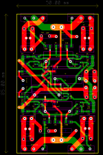
Here's an initial PCB design for the last schematic I posted, with the addition of some supply bypass caps and Zobel networks, if needed. The four very large components in the middle are daughterboards for the current sources and output stage bias voltages, which were mentioned in another thread. Along with using mostly SMT components it helps keep the board fairly compact. It could probably be a lot smaller if I put more components on the other side, but I think my head would burst trying to route it. Output devices are plastic TO3P types, two each end. I haven't checked it for errors, so don't even think about making one!
One potential problem with the circuit as last shown is that the maximum Vgs of the output devices could be exceeded. Output stage voltage could be increased to 20-25V to fix that, with little loss of rail efficiency (current capability of the output devices would need to be quite large though).
One potential problem with the circuit as last shown is that the maximum Vgs of the output devices could be exceeded. Output stage voltage could be increased to 20-25V to fix that, with little loss of rail efficiency (current capability of the output devices would need to be quite large though).
Attachments
Hi all,
I'm beginning about folded cascodes. For the momment it's not symmetrical, but I'm trying to make it work.
Here's what I think to be a folded cascode. But how can I set it's bias point, and its gain?
I mean, what current though the diff pair, what current though the cascode transistors, what base voltage....
Thanks
Folded Cascode
http://www.diyaudio.com/forums/showthread.php?s=&threadid=1794&highlight=

Bricolo said:Hi all,
I'm beginning about folded cascodes. For the momment it's not symmetrical, but I'm trying to make it work.
Here's what I think to be a folded cascode. But how can I set it's bias point, and its gain?
I mean, what current though the diff pair, what current though the cascode transistors, what base voltage....
Thanks
http://www.diyaudio.com/forums/showthread.php?s=&threadid=1794&highlight=
From what I inderstood, folded cascode work this way:
You have a classical diff pair front end made of a common emitter (for BJTs) transistor. They share the same current source at theyr emitters, and have collector resistors.
Now the difference is that emitters of common base transistors are also connected to the collector resistors of the front end.
So, to keep it short, the CE and CB transistors share the current flowing through the top resistors. When the CE sees a big input signal, it draws more current, so the CB recieves less current. Some kind of complementary current sharing.
Is this correct so far?
Are the current mirrors under the CB transistors required? I don't remember any folded cascode scematic without them.
But there are 2 folded cascodes designs I don't understand.
-The pass A75, the folded cascode topology isn't obvious, it seems much different from the one I tried to explain.
-Rudolf's super pair IV, made of a folded cascode, but with a resistor between the 2 super pair transistors, I don't unserdtand its role. But the IV doesn't work without it.
Bricolo said:
Are the current mirrors under the CB transistors required? I don't remember any folded cascode scematic without them.
Hi !
If you want at least some more gain you should use the currentmirror.
If you don't use it, you can skip the "left" half of the folded cascode.
The "ratio" between current of diffamp and FC set's most of the gain.
But think of FC more like "mirroring" down the output from diffamp.
Mike
Your analysis is correct. At the front you have a common-emitter transistor (usually two of them in long-tailed pair configuration) which reflects a current into a common-base transistor (again, usually two of them - one for each of the two common-emitter transistors via a current source (a simple resistor in all the amps here).
The current mirror is not strictly necessary. It's exactly the same as a current mirror often put on top of a long-tailed pair, but because it's a folded topology, it appears down the bottom instead. It increases gain and helps keep the two sides balanced. You'll notice that my design has no current mirror")
There are many possible ways to make a folded cascode, the important parts are the CE transistor, current source and CB transistor. Op-amps using folded cascode topology tend to have a lot more transistors in them, whereas discrete designs tend to use more resistors. I can't comment on the two particular designs you mentioned because I haven't seen them. If you link to some schematics I can see if I understand them.
The current mirror is not strictly necessary. It's exactly the same as a current mirror often put on top of a long-tailed pair, but because it's a folded topology, it appears down the bottom instead. It increases gain and helps keep the two sides balanced. You'll notice that my design has no current mirror
There are many possible ways to make a folded cascode, the important parts are the CE transistor, current source and CB transistor. Op-amps using folded cascode topology tend to have a lot more transistors in them, whereas discrete designs tend to use more resistors. I can't comment on the two particular designs you mentioned because I haven't seen them. If you link to some schematics I can see if I understand them.
Bricolo, does this help?
http://www.diyaudio.com/forums/showthread.php?postid=119592#post119592
I prefer to use active current sources rather than collector resistors.
regards, jonathan carr
http://www.diyaudio.com/forums/showthread.php?postid=119592#post119592
I prefer to use active current sources rather than collector resistors.
regards, jonathan carr
Pass A75:Mr Evil said:I can't comment on the two particular designs you mentioned because I haven't seen them. If you link to some schematics I can see if I understand them.
http://www.passdiy.com/pdf/A75p1.pdf
Last chapter in page 6, and schematic in page 7
Super Pair IV:
http://www.diyaudio.com/forums/showthread.php?threadid=25051
look at R26
Ok, the Pass A75: Most of the components are biasing circuitry. Taking only the top half for example, Z1 and R11 form the bias voltage for the cascode transistor Q9 and also biases Q7 which is used as a current source for the lower differential. R17 and R19 are presumably there for stability. Q3 is the current source reflecting the current from the differential into the cascode, but it is modulated by the signal from the other half of the differential. As the documentation says, choosing different values of resistors can make Q3 dominate, behaving like a normal Vas, or Q9 as a cascode.
As for the super-pair: I'm having a difficult time seeing quite how that works.
As for the super-pair: I'm having a difficult time seeing quite how that works.
- Status
- This old topic is closed. If you want to reopen this topic, contact a moderator using the "Report Post" button.
- Home
- Amplifiers
- Solid State
- Symmetrical folded cascode.