It's quite difficult to properly solder (or desolder) a pad that is connected to a plane,
without using them. They are universally used in pcb design.
https://en.wikipedia.org/wiki/Thermal_relief
https://www.google.com/search?q=the...zmmorMAhWFJCYKHfd2CrUQsAQIIw&biw=1093&bih=506
Depends on the supply current, where possible it is best to use them, but some designs just have too much current.... To give an assembler a challenge I did some boards for a BIG SMPS (13kW) using 4 and 6 ounce copper, NO thermal relief
")
The rule for high current is that the spokes width must be the trace width for the required current divided by the number of spokes. (Ref IPC-2221, IPC-2152 etc.)
@AndrewT
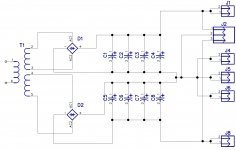
This is the schematic.
Like I said on the 1st post, I have 2 rectifiers.
Each has 4 caps.
1st cap on each is directly tied to rectifier on all my PCBs except the last one.
This is the schematic.
Like I said on the 1st post, I have 2 rectifiers.
Each has 4 caps.
1st cap on each is directly tied to rectifier on all my PCBs except the last one.
Yeah. And I've seen some PCBs here which have enormous ground plane but they connect the pad with 4 silly 0,33mm spokes.marce said:Depends on the supply current, where possible it is best to use them, but some designs just have too much current.
Attachments
I would use both wires for both psus. The differences - not the voltage-high only - between (+) and (-) would be more slightly.
It would sound a little bit cleaner, finer.
Not sure what you mean.
PSU is exactly as it is on schematic...it's +-56VDC.
Figured you will complain about Y.
GND plane overlaps both + and - plane, look closer, on both 2.4 and current 2.5 version.
If I have to look closer to see, then they don't. 100 % overlap is needed, not a fraction of a mm. It's practically nothing. And I repeat, it should be continuos.
Why to ruin something that has been almost perfect?
You mean one rectifier and 4 caps for each amp?"One" rectifier,-)
Because I don't like it. I'll make another version.Pafi said:If I have to look closer to see, then they don't. 100 % overlap is needed, not a fraction of a mm. It's practically nothing. And I repeat, it should be continuos. Why to ruin something that has been almost perfect?
Yeah. And I've seen some PCBs here which have enormous ground plane but they connect the pad with 4 silly 0,33mm spokes.
And do you think there is any problem with 4*0.33 mm spokes? What current do you want to use it for? Over 10 amps/capacitor? Do you think your capacitor survives 10 amps continuously? I tell you: it wont. But a single 0.33 mm track with 0.4 mm length can carry 10 amps easily. And that spokes has much lower impedance then anything else on your design. So no reason for you to avoid them.
Not every design needs thermal relief. For example in a 500 kHz DC/DC converter with 100A 1V output the inductance of a thermally reliefed pad can be too much, so it's better to be avoided. But it will be assembled in reflow owen, so no problem with any plane connected, everything is heated the same time.
Do you have a stereo amp = 2 amps? Complememtary-amps, (+) and (-) seprated, = 2 amps per channel: ergo 2 x 2 = 4 amps?
Than, if one trafo with two secondary-windings, one rectifier and 2 times xx caps. xx for one time (+), xx for one time (-).
Never ever channel separated psus,-!!!
Never,-! (Use better speakers and sources,-)
Than, if one trafo with two secondary-windings, one rectifier and 2 times xx caps. xx for one time (+), xx for one time (-).
Never ever channel separated psus,-!!!
Never,-! (Use better speakers and sources,-)
Because I don't like it. I'll make another version.
Then don't ask how to do it!
@AndrewT
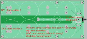
But I'm using 2 rectifiers! Not one!
I don't have one middle transformer point, I have 2 middle points.
Transformer has 4 wires. Yes, I could put middle ones together into one, but the idea is to use 2 rectifiers. So each rectifier has it own caps, first rectifier has upper capacitors, second has lower capacitors. Should they not connect on one single point at the end?
They can, but it increases the impedance. If you want it suboptimal, then do it this way! Actually I'm sure you will be satisfied with it. It's not bad, only not as good as could be.
You should have attached your complete schematic in 1'st post. (I don't know what you linked, I can't see them.)
And do you think there is any problem with 4*0.33 mm spokes? What current do you want to use it for? Over 10 amps/capacitor? Do you think your capacitor survives 10 amps continuously? I tell you: it wont. But a single 0.33 mm track with 0.4 mm length can carry 10 amps easily. And that spokes has much lower impedance then anything else on your design. So no reason for you to avoid them.
Yes I do. You try to achieve the "perfect" board with minimal impedance and then you ruin it with 1,32mm wire connected to pad? Seriously? Then all wires could be 1.32mm wide, why bother? Yeah yeah, spokes are just 2mm long, but I would rather use 4 spokes with at least 2mm width for each. If I wanted a fuse, I would have added it.
There sure are caps who can survive more than 10A continuously, just not the ones I'm using.
I didn't ask you directly, you replied by yourself.Pafi said:Then don't ask how to do it.
Do you hold any degree in electronics?
Do you work professionally as an electric engineer?
Because if you do, you should be aware that if I connect all caps with very thick wire, it will make no difference how it's connected, it will still work and it will absolutely in no way affect sound quality. Most people are just being subjective too much.
I value your opinion and I'm grateful for your help. Only point is that I've gotten different responses from different people. And I've read different articles who say different things, it's hard to conclude who is right and who is wrong mostly because the damn thing will work no matter how you connect it. Only if you mess it up real hard, you will have problems.Pafi said:They can, but it increases the impedance. If you want it suboptimal, then do it this way! Actually I'm sure you will be satisfied with it. It's not bad, only not as good as could be.
Also, I don't understand how it increases the impedance now? It's the same, absolutely the same schematic and PCB on all versions except the last. Did you even look at the images? Forget the last one which is totally different. On all PCBs there were 4 points for input, there was one point in which GND connects to one point Y. What exactly is wrong with it now? PCB on post 22 is THE SAME as the all others, except the fact that the last version does not have GND all over the + and - rails, which I will fix.
I guess you and I are not on the same page from post #1.
Should I use just one rectifier then and connect all caps to a single GND plane?
Had no idea images could be attached on this forum like that. You should have looked few posts below.Pafi said:You should have attached your complete schematic in 1'st post. (I don't know what you linked, I can't see them.)
Sorry, I just don't understand you. Your English is not the best I've seen but no matter that, I just don't get what you are saying.cumbb said:Do you have a stereo amp = 2 amps? Complememtary-amps, (+) and (-) seprated, = 2 amps per channel: ergo 2 x 2 = 4 amps?
Than, if one trafo with two secondary-windings, one rectifier and 2 times xx caps. xx for one time (+), xx for one time (-).
Never ever channel separated psus,-!!!
Never,-! (Use better speakers and sources,-)
Can you draw what you mean and attach it here?
Yes, I have 2 amps, stereo configuration.
Yes, I have a transformer with dual secondary windings.
Attachments
Last edited:
Hi Abdiel,
It is hard to help you. You've asked for help, you've got some hints. In post 22 you have a nice layout where I agree with Pafi. But yet in post 25 you changed it to a less optimum one. The difference you overlook is that in post 22 you have a ground plane which is lost in post 25 design. You've also introduced unnecessary cuts in the top layer GND pour between J1 and J3 (also J5 and J6) connectors in the design in post above which aren't doing anything good. You are right, all of your board designs would "work" and most probably you would not notice a difference, but this is not the point. It's just that for some reason given a chance to do something in an optimum way by following an advice, you choose a sub-optimum solution based on arguments which aren't clear. Also your arguments against thermal relief around the pads aren't reasonable.
Like it or not but you seem to have not understood the topic you are trying to argue about. I am not saying that I am and expert but there is a common knowledge in circuit design which you are trying to question.
Also, what would you say if Pafi actually is an electrical engineer or even holds a PhD in a dedicated field? I would think twice before starting to challenge the level of qualification of forum members. I agree with Pafi, why would you ask here for and advice if you "know better" anyway?
Regards,
Oleg
Hi Abdiel,
It is hard to help you. You've asked for help, you've got some hints. In post 22 you have a nice layout where I agree with Pafi. But yet in post 25 you changed it to a less optimum one. The difference you overlook is that in post 22 you have a ground plane which is lost in post 25 design. You've also introduced unnecessary cuts in the top layer GND pour between J1 and J3 (also J5 and J6) connectors in the design in post above which aren't doing anything good. You are right, all of your board designs would "work" and most probably you would not notice a difference, but this is not the point. It's just that for some reason given a chance to do something in an optimum way by following an advice, you choose a sub-optimum solution based on arguments which aren't clear. Also your arguments against thermal relief around the pads aren't reasonable.
Like it or not but you seem to have not understood the topic you are trying to argue about. I am not saying that I am and expert but there is a common knowledge in circuit design which you are trying to question.
Also, what would you say if Pafi actually is an electrical engineer or even holds a PhD in a dedicated field? I would think twice before starting to challenge the level of qualification of forum members. I agree with Pafi, why would you ask here for and advice if you "know better" anyway?
Regards,
Oleg
I never said I know better.
I will always ask "who are you and what is that you do" when I wish to judge the given answer. If person is qualified, I will listen. Common sense.
I went back to design on post #22 since Pafi said it's the best. I wanted to remove some things and put + and - fastons closer to GND. I'll soon post an update based on his words.
I sure hope he has a PhD, I would be very happy about it! I'm sick of subjectivism and all the crap I've read and seen, finally someone who can give the right answers.
@Pafi
I guess my words were misunderstood. When I said I'll do another design, I meant I wish to change some things based on design on post #22. Not "I'll do it better than you". If I knew better, I would have not asked.
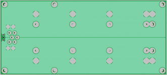
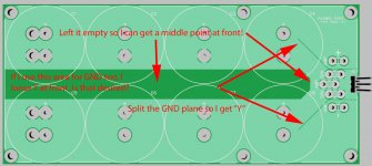
Anyways, I've made a new design. Removed cap/resistor for chassis, put + and - fastons closer to GND.
I've also reverted back + and - lines(bottom layer) so they are very close to each other as on post #22, which was intended. I also put GND plane on whole top layer, except in the middle.
As you can see, I left a bit of space in the middle and I've split the GND plane where connectors are so I can get an "Y".
Is this desired or not?
You said I should keep Y, but on one of the posts you said I should minimize the loop for first capacitor, which is what I have now, for both + and - planes, each plane's 1st capacitor returns directly to rectifier. Or am I mistaken here?
This is where you have confused me.
I'll do which is best.
I can also use 1 rectifier and then the entire top layer as GND makes sense to me perfectly. I'm just confused because it seems nobody understands what I'm trying to do, use 2 rectifiers.
I apologize if I offended anyone on any way.
I guess my words were misunderstood. When I said I'll do another design, I meant I wish to change some things based on design on post #22. Not "I'll do it better than you". If I knew better, I would have not asked.
Anyways, I've made a new design. Removed cap/resistor for chassis, put + and - fastons closer to GND.
I've also reverted back + and - lines(bottom layer) so they are very close to each other as on post #22, which was intended. I also put GND plane on whole top layer, except in the middle.
As you can see, I left a bit of space in the middle and I've split the GND plane where connectors are so I can get an "Y".
Is this desired or not?
You said I should keep Y, but on one of the posts you said I should minimize the loop for first capacitor, which is what I have now, for both + and - planes, each plane's 1st capacitor returns directly to rectifier. Or am I mistaken here?
This is where you have confused me.
I'll do which is best.
I can also use 1 rectifier and then the entire top layer as GND makes sense to me perfectly. I'm just confused because it seems nobody understands what I'm trying to do, use 2 rectifiers.
I apologize if I offended anyone on any way.
Attachments
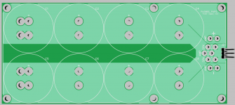
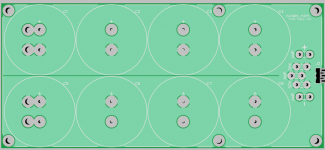
And this would be the updated version.
Left a small gap in the middle so GND is covering 100% of - and + planes.
Removed those splitters, this is still a Y connection, just with bigger joining point.
Bottom layer is the same, + and - planes on each half, very close to each other.
I've also used thermal reliefs(2mm per spoke), since all planes (+, -, GND) have very large areas.
Is this ok?
Attachments
Last edited:
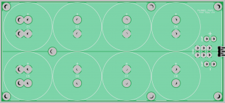
Your last pcbs are chaos-grounds. X- undefined circuits, currents.
I suggest the pcb # 53, with a little alteration as shown. To get not ground-loops, to get a more defined circuit, current.
And I would connect the middle-windings of the trafo, use one rectifier, to reduce the differences between (+) and (-). The minimal better pcb (would be) as shown below.
I suggest the pcb # 53, with a little alteration as shown. To get not ground-loops, to get a more defined circuit, current.
And I would connect the middle-windings of the trafo, use one rectifier, to reduce the differences between (+) and (-). The minimal better pcb (would be) as shown below.
Attachments
Your last pcbs are chaos-grounds. X- undefined circuits, currents.
I suggest the pcb # 53, with a little alteration as shown. To get not ground-loops, to get a more defined circuit, current.
And I would connect the middle-windings of the trafo, use one rectifier, to reduce the differences between (+) and (-). The minimal better pcb (would be) as shown below.
Chaos grounds? Nice name for a movie.
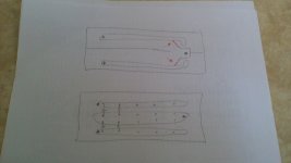
Ok, PCB from post #53...so I just cut more on top of pcb GND layer to create better Y. Ok, I'll do that because it has sense. Someone before you told me that that was not necessary... Oh boy, this is so confusing.
Your image, bottom part has GND in the middle. Pafi said not to do it that way, + and - planes should be as close to each other with GND plane only on top. I've also gotten the same response from another engineer(not from here). I'll wait what Pafi has to say.
Like I said before, one person tells me one way, other person tells me the other way. It's hard to know which is the "best".
- Status
- This old topic is closed. If you want to reopen this topic, contact a moderator using the "Report Post" button.
- Home
- Amplifiers
- Power Supplies
- Supply for amps - help with pcb