just because lots make the same mistake does not make the practice right.
Adding capacitance across the rectifiers just changes the frequency of the ringing.
A snubber is a resistance that absorbs the ringing energy.
A capacitor is not a snubber.
And you are correct on this one.
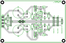
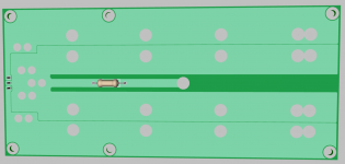
Removed the "snubber" caps. Added snubber network(R+C).
Any ideas for the values? I've put 10ohm and 220nF for now.
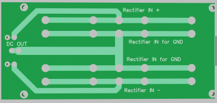
Attached the new pcb.
Thank you!
No no, just give me some text to read and some images to see for reference, I'll learn.Pafi said:Sorry, I don't have that much time! On 2 layers its easy, on 1 layer almost impossible.
Yeah, you are correct.Pafi said:The opposite is true. 0 distance is needed to achieve 0 inductance. They should be as close as possible!
Hm... I think I can do that. I'll try and post the result.AndrewT said:The tracks lying one above the other on a two sided PCB could be termed close.
Using a 1mm thick PCB would be better than using the standard 1.6mm thick PCB. Multi-layer PCBs that use ground and power planes properly have layer spacing of ~0.2mm
If you had a pair of dual polarity traces lying side by side on the bottom layer and the Zero volts track of twice the width on the topside and directly above them, you would get low EMI and low inductance.
Attachments
AndrewT said:The tracks lying one above the other on a two sided PCB could be termed close.
Using a 1mm thick PCB would be better than using the standard 1.6mm thick PCB. Multi-layer PCBs that use ground and power planes properly have layer spacing of ~0.2mm
If you had a pair of dual polarity traces lying side by side on the bottom layer and the Zero volts track of twice the width on the topside and directly above them, you would get low EMI and low inductance.
Not sure if something like this is what you had in mind...

Attachments
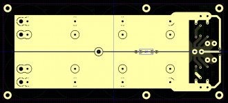
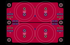
With this layout you achieved such a low impedance that now the RC+C snubbers can not shunt anything, they can be moved to the amp PCB. To the space become free you can move the power connectors, close to each other.
Now you have a difficult task with wiring, not to degrade the good quality you achieved within the PSU. ;-)
Really?
Ok, lemme see if I can upgrade it some more.
I will want your opinion on it again! ;-)
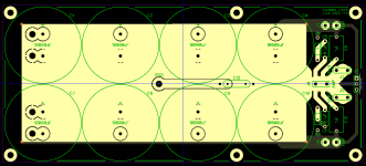
How about now?
Remember to use thermal reliefs for pads connecting to the plane.
Last edited:
Remember to use thermal reliefs for pads connecting to the plane.
I would rather not use them...
Are they really that necessary and if yes, why?
I would rather not use them...
Are they really that necessary and if yes, why?
It's quite difficult to properly solder (or desolder) a pad that is connected to a plane,
without using them. They are universally used in pcb design.
https://en.wikipedia.org/wiki/Thermal_relief
https://www.google.com/search?q=the...zmmorMAhWFJCYKHfd2CrUQsAQIIw&biw=1093&bih=506
Last edited:
Just an example
Hi,
Some time ago I've designed the attached boards for myself. I've made them and used them without problems.
Bottom layer is exact copy of the top layer. The GND is not created on the board by default but can be made by bridging the GND tabs with fast-on connector which becomes your star ground as well. Plus and minus are as depicted. The board accepts fats-on connectors or 5.08 mm pitch screw terminals for plus and minus, and also for the GND tabs. PCBs are symmetric so they can be attached to the rectifier bridge or the load from either side. You can also daisy-chain or stuck-up the boards by using wires or low value resistors and create a CRC supply. Bleeder resistors are on the underside. Many possibilities with these simple boards. Their size is 100x80 mm.
May be it will give you some ideas. Also do not overlook the need for easy access to the input connectors. Once you solder in the caps you will have hard time to solder/desolder the input wires...
Regards,
Oleg
Attachments
Remember to use thermal reliefs for pads connecting to the plane.
You have to set your iron to very hot and do a massive amount of pre-heating of the plane to get a successful soldered joint. That pre-heating can/will damage components.I would rather not use them...
Are they really that necessary and if yes, why?
Use Thermal reliefs. Many software packages can include them around pads.
Even with thermal reliefs you still need to use a hotter than usual iron and do a bit of preheating.
I often pre-solder the pad (don't fill the hole) before adding the component. That allows a quicker joint and thus less component heating.
Last edited:
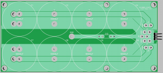
Figured you will complain about Y.pafi said:The previous was much better. GND plane should overlap both + and - tracks, and should be continuous in Y direction. As was.
GND plane overlaps both + and - plane, look closer, on both 2.4 and current 2.5 version.
@OlegSh
Yes, that's kinda what I'm trying to achieve but on single board.
Naaah, I'll solder the thing without problems, no need for relief pads. But I'll think about it.
Attachments
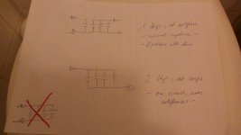
My suggests:
For max specify use hardwire, solid core, not pcb-flat-copper.
Most MAX. 1,5 mm!!! No doubling per solder!!!
Left picture:
If problems with hum the straight arrayed connection, as shown above.
If not, than general the circuit-correct connection, as shown below. Sounds much much cleaner!
Right picture:
Most ("double", + and -, complementary) one-step-psus or last step, after R or L or active step. (Your psu as example.)
Use the same types, the same values for max homogenity and cleanness. Minimum 3 - 4 caps.
No bridging little wonders,-!
My suggests,-)
Attachments
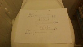
Not soooo much possibilities,-)
Just try a lot. Set some same caps as shown and connect different, as shown (included a hint to producers, engineers, how to construct caps and tubes, and how NOT to construct,-) - left picture. And listen. Listening-measurement. Not looking-measurement,-)
If you use a big pot - these sound scratchy and rumbling - than bridging per two ways. Right picture.
Further: how to set paralleled parts generally, active too,-!
Decide after, later,-)
Attachments
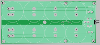
Not good. Go back to post22.Figured you will complain about Y.
GND plane overlaps both + and - plane, look closer, on both 2.4 and current 2.5 version.
@OlegSh
Yes, that's kinda what I'm trying to achieve but on single board.
Naaah, I'll solder the thing without problems, no need for relief pads. But I'll think about it.
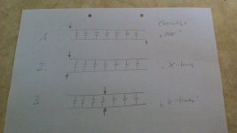
Input at one end, output at opposite end.
Resolve the charging pulse into the FIRST capacitor in the group at the INPUT. By the time the last capacitor of the group gets charged it is almost DC and this causes least interference to exit at the output.
Not good. Go back to post22.
Input at one end, output at opposite end.
Resolve the charging pulse into the FIRST capacitor in the group at the INPUT. By the time the last capacitor of the group gets charged it is almost DC and this causes least interference to exit at the output.
My last schematic and post 22, they are the same. Inputs and outputs are on the same spot on both schematics.
I think that idea is for all caps to work the same and not to split the rectification(voltage smoothing) work. Did you maybe check BoraOmega website?
-> AUDIO - POMOCNI UREDJAJI - Izvori napajanja - Izvori napajanja u audio tehnici
:::Borina Amaterska Svastara:::
NEPRAVILNO - Incorrect
PRAVILNO - Correct
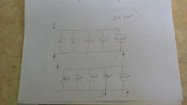
If I would be asked, I would go with this schematic. It would be even better to take currents from middle of the first 2 and last 2 caps and then join them in the middle so you get 2 by 2 parallel caps, same currents for all caps. I'll draw that later.
IMHO.
Attachments
If I am reading post 22 correctly it has a continuos Zero Volts plane under BOTH +ve and -ve rails.
It's this continuous plane that carries the charging pulses back to the transformer Centre tap.
Do not split the Zero Volts plane and force the returning charge current to go all the way to the OUTPUT end before returning to the transformer.
Keep the transformer/rectifier/firstcapacitor LOOP as short and compact as possible.
That does not keep LOW LOOP AREAS. It is a bad layout.I would go with this schematic. It would be even better to take currents from middle of the first 2 and last 2 caps and then join them in the middle so you get 2 by 2 parallel caps, same currents for all caps.
If I am reading post 22 correctly it has a continuos Zero Volts plane under BOTH +ve and -ve rails.
It's this continuous plane that carries the charging pulses back to the transformer Centre tap.
Do not split the Zero Volts plane and force the returning charge current to go all the way to the OUTPUT end before returning to the transformer.
Keep the transformer/rectifier/firstcapacitor LOOP as short and compact as possible.That does not keep LOW LOOP AREAS. It is a bad layout.
@AndrewT
But I'm using 2 rectifiers! Not one!
I don't have one middle transformer point, I have 2 middle points.
Transformer has 4 wires. Yes, I could put middle ones together into one, but the idea is to use 2 rectifiers. So each rectifier has it own caps, first rectifier has upper capacitors, second has lower capacitors. Should they not connect on one single point at the end?
Generally I don't use a PSU PCB.
I prefer to hardwire using twisted pairs everywhere.
One cannot achieve the equivalent interference attenuation using untwisted pairs, or big loop areas, that often get incorporated in a PCB.
Actually you can, broadside coupled tracks, been done for years on PSU designs, also called Bus Bar routing.....
Hence a ground plane or ground tracks under the positive rails instead of the silly spiders legs schemes I've seen on here... Just reading the whole thread so may have more comments
Last edited:
- Status
- This old topic is closed. If you want to reopen this topic, contact a moderator using the "Report Post" button.
- Home
- Amplifiers
- Power Supplies
- Supply for amps - help with pcb