Hi all! ")
In the past few months I've been working on a large DIY project consisting of amps, pre-amps, volume and tone controls, etc...
If all goes well, I'll put some photos of finished product within few months.
I've created schematics and PCBs for supplies, could somebody please check them and write if something is wrong or there is a better way of doing something there?
Size of the PCB can't be changed(enclosure limitations).
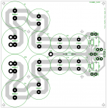
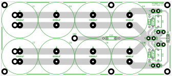
Amplifier PSU schematic/PCB:
https://cdn.pbrd.co/images/2W3FvKM.png
https://cdn.pbrd.co/images/2Wh1d8R.png
Note: using 2 diode bridges, 35A which are not on the schematic.
Is this the right way of connecting multiple caps with different values?
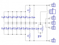
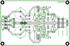
Pre-amplifier PSU schematic/PCB:
https://cdn.pbrd.co/images/2WnAp4e.png
https://cdn.pbrd.co/images/2WpOUXw.png
Any help is appreciated!
(I also offer a beer for any help from Croatian speaking members! )
)
In the past few months I've been working on a large DIY project consisting of amps, pre-amps, volume and tone controls, etc...
If all goes well, I'll put some photos of finished product within few months.
I've created schematics and PCBs for supplies, could somebody please check them and write if something is wrong or there is a better way of doing something there?
Size of the PCB can't be changed(enclosure limitations).
Amplifier PSU schematic/PCB:
https://cdn.pbrd.co/images/2W3FvKM.png
https://cdn.pbrd.co/images/2Wh1d8R.png
Note: using 2 diode bridges, 35A which are not on the schematic.
Is this the right way of connecting multiple caps with different values?
Pre-amplifier PSU schematic/PCB:
https://cdn.pbrd.co/images/2WnAp4e.png
https://cdn.pbrd.co/images/2WpOUXw.png
Any help is appreciated!
(I also offer a beer for any help from Croatian speaking members!
)You don't have any pics attached.Pictures are attached.
You have used a remote server
No, I can only see links to https.Can't you see them?


Hi Abdiel,
Even though you provide no details regarding the amp and the pre-amp you are going to power with your PSUs, I see unnecessary waste of PCB area in your designs. Could you explain why did you use 10000||10000||6800||6800||4700||4700 uF combination for the amp PSU instead of paralleling four 10000 uF caps which would be more compact? Have you actually looked at the existing designs, e.g universal PSU from diyaudio store? Also C||RC snubber after the capacitor bank should probably be put before the rectifier according to Mark Johnson. On the pre-amp PSU I would turn the regs parallel to the board's edge and make provision for the heatsinks. Also what is the purpose of D4 and D5 on the pre-amp PSU? You could look on ebay which is full of LM317/LM337 PSU PCBs... even if just for an inspiration.
Just my two cents...
Oleg
I've linked to another web source.
You have to click the link to see the image.
Same on the 1st post.
http://img.photobucket.com/albums/v280/cythlon/AMPS/pre_sch.png
http://img.photobucket.com/albums/v280/cythlon/AMPS/pre_pcb.png
http://img.photobucket.com/albums/v280/cythlon/AMPS/amp_sch.png
http://img.photobucket.com/albums/v280/cythlon/AMPS/amp_pcb.png
Abdiel, it is a reasonable request when members ask you to use our servers to host schematics and artwork. This prevents them from disappearing and rendering the thread meaningless in the future. Someone may find your your efforts informative in the future.
They are attached.
They are attached.
Attachments
When designing a PS you should create ground reference point. This is the point that interconnects all grounds from different boards. See the attached pictures for a simple example.
I do have it. Look closely.
2 MOSFET amps from ESP, P101. Hi powered versions. Transformer is 600VA so I could get above 150W on each amp.Hi Abdiel,
Even though you provide no details regarding the amp and the pre-amp you are going to power with your PSUs, I see unnecessary waste of PCB area in your designs.
Waste of PCB can't be avoided in my case so just bear with me.
The idea was to use larger and smaller caps since smaller ones charge and discharge quicker than the large ones.Could you explain why did you use 10000||10000||6800||6800||4700||4700 uF combination for the amp PSU instead of paralleling four 10000 uF caps which would be more compact?
Unfortunately I bought all the caps before I realized I will have to make this kind of messy PCB for it. I still can use 8x10000 caps but then smaller ones will be left unused(something I would like to avoid).
Sure I did. Along with numerous others.Have you actually looked at the existing designs, e.g universal PSU from diyaudio store?
Rectifier bridges have their own snubbers. According to Texas Instruments "AN-1849 An Audio Amplifier Power Supply Design" C||RC snubbers are welcomed after big capacitor banks due caps inductance.Also C||RC snubber after the capacitor bank should probably be put before the rectifier according to Mark Johnson.
Putting regulators on board edges is a no go for this PCB, but I will make some space for the heatsinks. Thnx!On the pre-amp PSU I would turn the regs parallel to the board's edge and make provision for the heatsinks.
ESP (sound westhost...) site could probably tell you more, I've read it months ago and if I remember it correctly D4 and D5 are for some kind inductance... Well, I can remove them easily.Also what is the purpose of D4 and D5 on the pre-amp PSU? You could look on ebay which is full of LM317/LM337 PSU PCBs... even if just for an inspiration.
Just my two cents...
Oleg
Abdiel, it is a reasonable request when members ask you to use our servers to host schematics and artwork. This prevents them from disappearing and rendering the thread meaningless in the future. Someone may find your your efforts informative in the future.
They are attached.
Not sure I understand how.
But I'll find out.
Thnx!
Since images tell 10000 words...
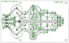
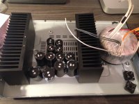
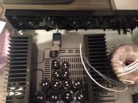
Amps go on each heatsink slightly toward the front. So I have to use the end of heatsinks for place to put large capacitors. After OlegSh post, I'm was thinking of using only 10000uF caps but I can't use 4 in a row, only 3 per row. ALPS 4 channel pot is coming in front of the pcb, at the center. To many space limitations.
You can see amp capacitors so you can image where amp psu pcb goes.
Pre amps psu pcb goes directly above it.
I've been messing with this for ages, no other way.
@kevinkr - found the info. Awesome!
Attachments
I found it good practice to keep power supply and amplifier/preamp separate.
I got caught out badly with a USB mixer I designed.
I just mixed in power supply and audio and got 1 volt peak 2 peak of hum !
The smoothing capacitor charging pulses were modulating the ground and feed into the audio path.
I redesigned the pcb keeping power supply separate and it worked very well.
Star zero volt line works well too.
Have one point for the zero volt lines to go to and keep them separate.
When designing a PS you should create ground reference point. This is the point that interconnects all grounds from different boards. See the attached pictures for a simple example.
Amasing how a very simple schematic can be turned into an extremely overcomplicated, still not good PCB. As you told GND is the most important potential in an amplifier, and despite of this we can see unneccessarily long, but thin (high impedance) traces in GND net, while a huge amount of copper is wasted for Earth. At least the charging current doesnt go through the star point (as the sch suggests). This is the only good point of the PCB. (However this is no. 1 importance.)
Maybe the 2nd most important thing is not to ruin ESR of capacitors. A good capacitor has about 10-20 mohm of ESR. Parallelled 5 has 2-4 mohm. 40mm track with 2mm width is 10 mohm. So if this track is in the loop, then the money spent on quality caps is thrown into the trash bin. In this aspect the topic starter PCB is a very bad design, since the big caps effectively cant work at high freq.
In a power converter PCB every place not covered by copper is a waste of money. Rails should be as wide as possible. If 2 layers are used, then 1 should be an almost continuous GND plane (small gaps may needed to control route of charging pulses to separate them from signal GND). Loop areas closed through different caps should not differ much.
Wire or PCB track?
Loop inductance of 2 typical wires side by side is about 1 uH/m. (Twisting doesnt help.) Two tracks side by side is about the same. Two 2mm tracks 1 over the another, on 2 sides is about the half, and 2 planes (on opposite sides of the same area, 10-20 mm wide) is almost 1 magnitude lower. Thin PCBs are even better in this aspect.
Why is this important?
Because a class AB amp has a very distorted supply current. This flows through supply loop, generates distorted voltage spikes, and finds its way to the output through not perfect PSRR of amp. The less the impedance the less the distortion generated 'by PCB'.
I will use 8x10000uF caps. After some additional measurement seems it will fit just about right.
PCB is attached.
I forgot to mention that I will use additional wire(1-2mm2)and connect capacitors with it(following the trace lines) for additional "copper".
Lines are 6mm wide on amp psu pcb.
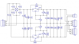
Thanks to JohnnyBerg I added a place for faston for common GND on pre-amp psu pcb. It was a simple pad before.
Image is attached.
@Pafi
Where the charging current should go then?
Not sure which schematic are you referring to...
I will lower the impedance of tracks by soldering additional wire along the tracks on pcb. I can also put the same tracks on 2nd layer which would double the width of the tracks to 12mm(6mm x2). In that case I would not use additional wire.
@AndrewT
@nigelwright7557
PCB is attached.
I forgot to mention that I will use additional wire(1-2mm2)and connect capacitors with it(following the trace lines) for additional "copper".
Lines are 6mm wide on amp psu pcb.
Thanks to JohnnyBerg I added a place for faston for common GND on pre-amp psu pcb. It was a simple pad before.
Image is attached.
@Pafi
I've made it less complicated.Amasing how a very simple schematic can be turned into an extremely overcomplicated, still not good PCB. As you told GND is the most important potential in an amplifier, and despite of this we can see unneccessarily long, but thin (high impedance) traces in GND net, while a huge amount of copper is wasted for Earth. At least the charging current doesnt go through the star point (as the sch suggests). This is the only good point of the PCB. (However this is no. 1 importance.)
Where the charging current should go then?
Not sure which schematic are you referring to...
I don't know how to make GND plane for this schematic that will "improve" sound/ESR/whatever... Could you show me on some example?Maybe the 2nd most important thing is not to ruin ESR of capacitors. A good capacitor has about 10-20 mohm of ESR. Parallelled 5 has 2-4 mohm. 40mm track with 2mm width is 10 mohm. So if this track is in the loop, then the money spent on quality caps is thrown into the trash bin. In this aspect the topic starter PCB is a very bad design, since the big caps effectively cant work at high freq.
In a power converter PCB every place not covered by copper is a waste of money. Rails should be as wide as possible. If 2 layers are used, then 1 should be an almost continuous GND plane (small gaps may needed to control route of charging pulses to separate them from signal GND). Loop areas closed through different caps should not differ much.
Can't make tracks side by side unless I widen the tracks... Shouldn't tracks be as far as possible so you get 0 H/m? Also, can't make tracks on top of each other in this case, so I'm not following. Sorry.Wire or PCB track?
Loop inductance of 2 typical wires side by side is about 1 uH/m. (Twisting doesnt help.) Two tracks side by side is about the same. Two 2mm tracks 1 over the another, on 2 sides is about the half, and 2 planes (on opposite sides of the same area, 10-20 mm wide) is almost 1 magnitude lower. Thin PCBs are even better in this aspect.
Why is this important?
Because a class AB amp has a very distorted supply current. This flows through supply loop, generates distorted voltage spikes, and finds its way to the output through not perfect PSRR of amp. The less the impedance the less the distortion generated 'by PCB'.
I will lower the impedance of tracks by soldering additional wire along the tracks on pcb. I can also put the same tracks on 2nd layer which would double the width of the tracks to 12mm(6mm x2). In that case I would not use additional wire.
@AndrewT
Why? Every single "serious" supply puts capacitors as snubbers on diodes... Even "low cost hi-fi" equipment have them.Remove C1 to C4. They are likely to make ringing on the supply lines worse.
Instead add an R+C snubber in parallel to C12.
@nigelwright7557
They are on separate PCBs. One is on top of other regarding positioning. I don't think that should cause problems since they will be separated enough. The problem is, I don't have anywhere else to put it.I found it good practice to keep power supply and amplifier/preamp separate.
Attachments
just because lots make the same mistake does not make the practice right.Why? Every single "serious" supply puts capacitors as snubbers on diodes... Even "low cost hi-fi" equipment have them.
Adding capacitance across the rectifiers just changes the frequency of the ringing.
A snubber is a resistance that absorbs the ringing energy.
A capacitor is not a snubber.
Last edited:
@Pafi
I've made it less complicated.
Where the charging current should go then?
Not sure which schematic are you referring to...
Not yours, but one of JohnnyBerg. PCB too. Yours is not complicated, and charging current goes on a mostly harmless way in both of your designs (if I decoded your design correctly, since you didn't indicate inputs at all).
I don't know how to make GND plane for this schematic that will "improve" sound/ESR/whatever... Could you show me on some example?
Sorry, I don't have that much time! On 2 layers its easy, on 1 layer almost impossible.
Can't make tracks side by side unless I widen the tracks... Shouldn't tracks be as far as possible so you get 0 H/m?
The opposite is true. 0 distance is needed to achieve 0 inductance. They should be as close as possible!
I will lower the impedance of tracks by soldering additional wire along the tracks on pcb.
It reduces resistance, but not inductance.
I can also put the same tracks on 2nd layer which would double the width of the tracks to 12mm(6mm x2). In that case I would not use additional wire.
A GND plane on second layer would be much better.
The tracks lying one above the other on a two sided PCB could be termed close.
Using a 1mm thick PCB would be better than using the standard 1.6mm thick PCB.
Multi-layer PCBs that use ground and power planes properly have layer spacing of ~0.2mm
If you had a pair of dual polarity traces lying side by side on the bottom layer and the Zero volts track of twice the width on the topside and directly above them, you would get low EMI and low inductance.
- Status
- This old topic is closed. If you want to reopen this topic, contact a moderator using the "Report Post" button.
- Home
- Amplifiers
- Power Supplies
- Supply for amps - help with pcb