Hi Juan,
I posted the sprint file in post #2132
Again it is Kuntarman's file but with a couple of my changes.
I'm about to ask you something lol the zip file didn't open what program are you using to opened ?
I'm about to ask you something lol the zip file didn't open what program are you using to opened ?
Someone else said that. I use 7-zip.
Someone said it is a rar file.
I will try again. See if the attached will open.
Attachments
good to go
good to go Terry thanks") I use a free version of WinRAR
I use a free version of WinRAR
Someone else said that. I use 7-zip.
Someone said it is a rar file.
I will try again. See if the attached will open.
good to go Terry thanks
I use a free version of WinRARAttachments
Terry,
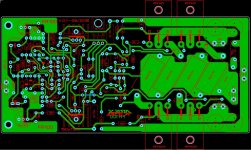
I do not see any show stoppers with the layout. I did not go over each connection against the schematic. That is what a full layout s/w package is supposed to do for you
have some text on the left intersecting a trace. "pcb by ..."
Put silk for polarity outside of comp body(silk) so you can identify/check after comp is inserted!
I do see that some traces have what would be considered pad exit violation, but that is nit picking.
Hope it works out for you.
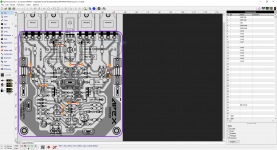
Hi,
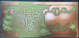
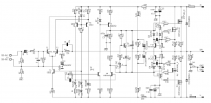
DOes pad exit violation mean very sharp corner between adjacent traces eatering a pad or trace entry centered on pad?
How does the attached example fare or do you see any such observations?
reg
prasi
Attachments

Nice.. layout Dacz,trial
D8 on red marked, i think inverted.

Regards, Kuntarman
Sent from my Coolpad 8297W using Tapatalk
FR100
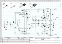
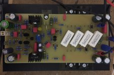
Hi, here is the next FR100. It sounds really good.
It runs at +- 50V with a total quiescent current of 100mA. The transistors of the input stage run quite hot. MPSA92 can be touched a maximum of 3...5 seconds, then it really hurts.
The layout is not optimal, but I wanted to mount it on this heatsink.
Thanks to Mile for this lovely amplifier.
regards Olaf
Attachments
Hi, here is the next FR100. It sounds really good.
It runs at +- 50V with a total quiescent current of 100mA. The transistors of the input stage run quite hot. MPSA92 can be touched a maximum of 3...5 seconds, then it really hurts.
The layout is not optimal, but I wanted to mount it on this heatsink.
Thanks to Mile for this lovely amplifier.
regards Olaf
Nice work,
Regards


Thimios a nice idea , it does not matter for me please edited as good as you'd like.Just an idea.
Sorry if my english is not good , I use google translate .
Sent from my Coolpad 8297W using Tapatalk
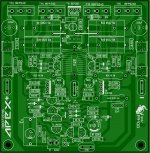
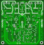
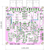
I made a layout for anyone who wants to create a prototype APEX FR50, sorry if there are mistakes, please correct.
View attachment 569908
View attachment 569909
View attachment 569910
Nice work,
Regards
Just got my SR-200 pcb done . The pcb is alex_mm Ver 3.2 with toshiba outputs . Can anyone guide me the testing procedure for the amp ? I will be completing one channel tomorrow and I will be testing it with a single pair of out transistors . I would like to know what I should be checking and I do not have access to a scope .
Nice layout design Prasi ,Ok, 5th option for FR-100.
Havent spent much time in it, just a quick one day affair
reg
Prasi
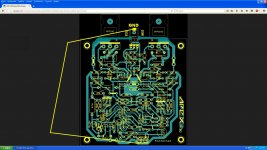
*please be corrected again in part (M2 IRFP9240) the red circle . I think the connection is reversed between pin D & S.


*Emitter T10 & T11 must connect with out/spk, please see Apex fr100 original sch.
Sent from my Coolpad 8297W using Tapatalk
Last edited:
- Home
- Amplifiers
- Solid State
- Studio Reference Amplifier