I read Charles' explanation of EquiLock and after waving the smoke aside concluded it was a cascode, such that Vec on the gain device was constant.
However, precisely IF the Vec on the gain device is a constant, then it's no longer a gain device....
So, I ask the Doris Day question, is that all there is?
Damn good figures, MB, hats off.
Hugh
However, precisely IF the Vec on the gain device is a constant, then it's no longer a gain device....
So, I ask the Doris Day question, is that all there is?
Damn good figures, MB, hats off.
Hugh
Thank you Aksa,
I'll soon publish the circuit after I've put in two more cascode transistors. Right now, 2 fets run way beyond their dissipation limit in the Sim, but good thing is that it doesn't simulate smoke")
As for your question, I think it's a gain device still as it's still capable of ampifying the input current, irregardless of the actual Vce drop, as long as it is enough. The emitter voltage of the cascoding transistor should never 'hug' the voltage of the collector of the gain device. You basically pin the gain device's behaviour on a given Vce. The 'variable collector potential' action is moved to the casoding device.
I'll soon publish the circuit after I've put in two more cascode transistors. Right now, 2 fets run way beyond their dissipation limit in the Sim, but good thing is that it doesn't simulate smoke
As for your question, I think it's a gain device still as it's still capable of ampifying the input current, irregardless of the actual Vce drop, as long as it is enough. The emitter voltage of the cascoding transistor should never 'hug' the voltage of the collector of the gain device. You basically pin the gain device's behaviour on a given Vce. The 'variable collector potential' action is moved to the casoding device.
Last edited:
Well, meanwhile I've made another bit of nice progress.. I was able to get rid of 5 watts of power dissipation and a number of transistors since a part of the VAS control could fit directly under it's positive side cascode. The VAS is quite elaborate, but even then, with a less optimized common mode reference it still works well - it's fully current based, despite FETs being transconductance amplifiers rather than current amplifiers like BJTs. It's close to being finalized now..
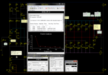
Attached a display of its approximate THD20. It's no joke. Once the schematic is done, the VAS may be less obscured
Attached a display of its approximate THD20. It's no joke. Once the schematic is done, the VAS may be less obscured
Attachments
MB,
Agree, but we are looking at semantics. The lower device is a current gain device, since input as at base and output at collector (common emitter). The upper device is a voltage gain device, since input is at emitter and output at collector (grounded base).
Miller effect will be absent from the lower device, of course, the whole point of a cascode. And the upper device will deliver wonderful bandwidth, again, the point of a cascode.
Even so, my preference for a cascode is a constant power type, of the type described by peufeu in his discussion of Lavardin distortion here:
Lavardin Distortion: Brainwashing the VAS
Cheers,
Hugh
Thanks, I'm still in the process of optimizing
I also dug up a link to my build log of the 80W symmetrical MOSFET amp I was talking about
Nice design, its very similar to a australian amp lineup except youve opted for darlington vas and and therefore better THD figures, square wave response looks very good too.
Since the design is built and tested you should present it here as well, there are many DIYers that prefer full symmetrical amps and there practically arent any here shown with full completion and PCB that they could build.
Interesting to see what you came up with this time, but I agree with you, with Fets its not to hard to equal and surpass amp performance compaired with BJTs.
Yeah, they require just that bit of different thinking than you would using BJTs. But I have to say that it is actual circuit topology that's the greatest contributor to performance, closely followed by choice of active devices. At least, that's my experience from averaging anecdotal results of trying all kinds of topologies and schematics. The cool thing of simming is that you can quickly analyse broadly the circuit for general improvement/degrading without the risk of blowing up parts. Cascodes and current mirrors are just building blocks, just as the LTP is. It's how you put it all together what makes the difference or not.
As for the VAS, I can already explain it's operation:
To have the VAS be controlled symmetrically in a push-pull fashion means that two current sources need to be controlled. The upper and lower VAS currents. The difference between those is what determines the voltage output of the VAS, amongt others.
The thing however, is that I have a single-ended push-pull input, the output of the left leg of the IPS, between the top FET that acts as a current mirror output, and the drain of the cascode FET. The 'free voltage' range of this output is between the saturation voltage of either FET. Naturally, if this output were balanced in the middle between those two voltages with a zero input signal, this would ofcourse be optimal - having the same 'room' both pos/neg swing.
So, this set a requirement. I want this single ended input fixed at a given target voltage optimal to the IPS output. What I created are two current valves to control those two VAS current sources in a balanced push-pull fashion. These current valves have a differential input and a common mode as wide as the supply range. So it was easy to bias the IPS idle voltage against an intended reference voltage. Iq is determined by one bias setting for the two valves. It's the VAS Iq bias. The bias resistor is easily insulated through capacitance as this is a fixed reference A JFet in the current loop determines the maximum VAS current allowed at all.
As for the VAS, I can already explain it's operation:
To have the VAS be controlled symmetrically in a push-pull fashion means that two current sources need to be controlled. The upper and lower VAS currents. The difference between those is what determines the voltage output of the VAS, amongt others.
The thing however, is that I have a single-ended push-pull input, the output of the left leg of the IPS, between the top FET that acts as a current mirror output, and the drain of the cascode FET. The 'free voltage' range of this output is between the saturation voltage of either FET. Naturally, if this output were balanced in the middle between those two voltages with a zero input signal, this would ofcourse be optimal - having the same 'room' both pos/neg swing.
So, this set a requirement. I want this single ended input fixed at a given target voltage optimal to the IPS output. What I created are two current valves to control those two VAS current sources in a balanced push-pull fashion. These current valves have a differential input and a common mode as wide as the supply range. So it was easy to bias the IPS idle voltage against an intended reference voltage. Iq is determined by one bias setting for the two valves. It's the VAS Iq bias. The bias resistor is easily insulated through capacitance as this is a fixed reference
A JFet in the current loop determines the maximum VAS current allowed at all.You now have my attention also, what are the latest updates, I would like to sim as we go as well.
Funny thing, I at first glance did not see much of interest except a bucket full of components arranged so that I did not immediately understood the careful thought that was being displayed there.
I was gently reminded (nudge) to go look carefully and so I did - it is rather unconventional and I am incurious to see where it ends.
Black Magic in the Box
Hi Nico,
Thank you for stopping by I plan to publish the the schematic today or tomorrow. I've finalized the circuit although it couldn't hurt to doublecheck stuff. It'll be a black on white clean schematic, with added voltage/current probes so people can get an idea of how its bias is when idle.
The final schematic isn't special in sub circuits used - the tracking cascode as I called the early VAS has been replaced by a push-pull mechanic so it hadn't a place any more. The new VAS however is still quite elaborate, its current circuit is a series of cascodes, a current mirror, and a single ended push-pull control input consisting of 4 FETs that cancel out each other's harmonics. I wonder what Bob would think of this concrete VAS implementation
Anyways tonight the final schematic should appear and we can start doublechecking it, see if there's still errors in there I have missed (dissipation), addition of 'best practice' decoupling etc.
That'll be compiled into a PCAD schematic from which I can start designing the PCB at a later point. Like my previous design, it will include an integrated driver supply using zener stacked LM317/337's that can be fed directly from the supply buffer cap output. It'll be awesome to start building the prototype
Thank you for stopping by
I plan to publish the the schematic today or tomorrow. I've finalized the circuit although it couldn't hurt to doublecheck stuff. It'll be a black on white clean schematic, with added voltage/current probes so people can get an idea of how its bias is when idle.The final schematic isn't special in sub circuits used - the tracking cascode as I called the early VAS has been replaced by a push-pull mechanic so it hadn't a place any more. The new VAS however is still quite elaborate, its current circuit is a series of cascodes, a current mirror, and a single ended push-pull control input consisting of 4 FETs that cancel out each other's harmonics. I wonder what Bob would think of this concrete VAS implementation
Anyways tonight the final schematic should appear and we can start doublechecking it, see if there's still errors in there I have missed (dissipation), addition of 'best practice' decoupling etc.
That'll be compiled into a PCAD schematic from which I can start designing the PCB at a later point. Like my previous design, it will include an integrated driver supply using zener stacked LM317/337's that can be fed directly from the supply buffer cap output. It'll be awesome to start building the prototype
No, I don't have a copy of his book. I've read a few snippets though. I wonder if his method is the same as or differs from mine. Maybe Bob has a public domain reference to said circuit for me to compare to?
Ill ask his permission to show his input section, I think its quite brilliant, I did a new design around it using pushpull folded cascode vas augmented with hawksford cascodes to achieve similar THD figures I get with my other vas in single end. Folded cascodes are excellent building blocks but to really make them come on song they should be cascoded, the only one that I find to really improve things with folded is the so called hawksford. Before I even start listening tests Ill have to get Bob permission to use his circuit or the whole exercise would be of no use to me.
It's okay to show in PM.. I'm just interested in whether the mechanic I came up with is similar in the way of thinking in context to the SOM design. If the circuit would be an improvement I'll have to buy one off Bob Personally I think the VAS circuit I came up with now would perform equally if not better as the circuit is in/out matched to both the IPS and OPS while still being able to use a singular OPS -> VAS feedback path. But tonight after I get home from work we'll see
Personally I think the VAS circuit I came up with now would perform equally if not better as the circuit is in/out matched to both the IPS and OPS while still being able to use a singular OPS -> VAS feedback path. But tonight after I get home from work we'll see Yea I know, I deliberatly covered the VAS as it was not finalized (FETs running out of spec, no optimization yet, just the topology that in itself increased performance magnitudes. I now managed to reduce VAS current and optimize biassing and transistor dissipation and still performs great. It's amazing getting sub-ppm consistently irregardless of bias variations. One 1W THD20 measurement resulted in 26ppb Now that isn't representative as with simulation, there's artifacts, simulated noise etc. so what I do is just log THD results and average over a broad range. I'd say that its full power THD20 is around 0.5ppm, 1W THD in the 50ppb region.
But in a few hours, I'll post the full schematic.
Now that isn't representative as with simulation, there's artifacts, simulated noise etc. so what I do is just log THD results and average over a broad range. I'd say that its full power THD20 is around 0.5ppm, 1W THD in the 50ppb region.But in a few hours, I'll post the full schematic.
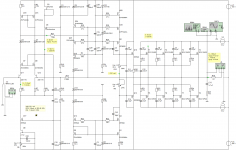
Well, here's the schematic The wire connecting dots are there, although not very clear. It's too bad I can't set them to be bigger in multisim.
It may look complex, but in reality it's very simple, I may draw a simplified operational diagram.
It's a big sized picture so take your time to glance over
The wire connecting dots are there, although not very clear. It's too bad I can't set them to be bigger in multisim.It may look complex, but in reality it's very simple, I may draw a simplified operational diagram.
It's a big sized picture so take your time to glance over
Attachments
I'll extract and post the models in a little while, although the ECX models I got from this very forum. I'll include them for completeness though.
C21 is the local feedback for Q17, it's mainly to mute any parasitic oscillation of Q17.
C22 is a bypass as you would place an electrolitic cap along a zener to get a cleaner voltage. Q6 with variable R5 forms the adjustable LTP current. C22 together with cascode Q17 protects Q6 from being modulated by the amp input. It's a highly steady currentsource this way.
I could replace R9 with a zener yes, but the rest of that current channel that is about 4mA wouldn't be changed; the idea here was to use a currentsource as input for the input cascode, allowing it to be referenced against the input JFET sources while maintaining good PSRR. As for the choice resistor vs zener it probably wouldn't matter in this particular location I suppose.
The OPS drivers Q10, Q13 run about 11.7mA bias, the needed voltage drop across the resistor really doesn't need to be high as the ECX' start conducting as early as 0.1V, so yeah I can imagine it gives the impression that a much larger current would be present
I forgot to mention that a few caps need an electrolytic parallelled, I omitted them in the sim to avoid the long time constants, but C22 needs a 10uF, C9 about 10uF as well, C1, C28, C15, C24 and all the other zener voltage regulators also. C11 and C12 need around 220u and 470u respectively.
Spice models of all FETs used attached to this post
Spice models of all FETs used attached to this post
Attachments
Last edited:
- Status
- This old topic is closed. If you want to reopen this topic, contact a moderator using the "Report Post" button.
- Home
- Amplifiers
- Solid State
- "State-Of-MOS": 200W Ultra Low Distortion Pure FET Amplifier