Magicbox, I havent yet studied your vas in detail but because there is such a close resemblance to mine I think some of the caracteristics will be the same. You should also look at the transconductance of the combination which I suspect is increased although there is a reduction of the miller effect too. This is the case with mine.
It is also called a Hawksford cascode, from quite some time back.
Hugh
Hi Hugh, is there an audio book or paper you haven't read?
Dont quite know why its called a Hawksford as Japanese manufacturers were using them in their amps a decade before Hawksford wrote that paper. Another member however pointed me to the original patent, TEK it was if I remember correctly. A couple of years in advance of the Japanese too.
Jonathan Carr pointed this to me, US patent 3423685D 1964, by Tektronix Inc.
Jonathan Carr pointed this to me, US patent 3423685D 1964, by Tektronix Inc.
Last edited:
Well kudos to you too mate.
What facetious attitude, I dont quite understand what youre on about so Ill leave it at that.
Anyway the design is much more interesting than where these posts are leading, dont you think ?? So lets rather pay attention to the design and see how a build goes.
agreed, moved to pm. resolution that is, not argument
the VAS is effectively not a Cascode
if you're already using higher V input stage supply why not make it enough higher for the Vds > 2x Vt condition that greatly reduces the Mosfet's parasitic C nonlinearity
Then what do you think it is? Could it be called quasi-cascode? After all, the topology certainly shares attributes with that of a classical cascode, notably that it keeps Vds of the upper FET stable under normal operating conditions. It may be noteworthy that the lower FET is actually bias'ed such way that the upper FET is not saturated, in the schematic it has about 4V across drain/source. When the input increases (lower voltage) the 'cascode' can't deliver any more current than the upper FET would allow. All the drive is doing is 'help' the lower FET to accomodate the increase in current by the upper FET whose Vds is now even more stable since the source of the lower FET isn't modulating as much as if it would be driven from a fixed reference. But I agree, it's not a classical cascode, yet it exhibits behaviour of one.
As for the Vds > 2xVth, the supply already accomodates for that condition - at least, for the IRF; not the upper transistor.
You'll find a black-on-white schematic attached to this post.
Could I impose and ask for another one? That one is hard to make out in parts, especially which wires connect and which ones cross over. I've had a go with LTspice but my version does not work - probably because I got a few connections wrong.
Perhaps instead you can look at the original schematic. There I've colored the wires. Not so much because I fancy a colorful schematic but to easily discover a multisim bug - it sometimes lumps nets together as one. Giving it a color I can quickly see which nets color along which are not supposed to be part of that net. It's annoying but it works. You can use the coloring to see which nets need to be connected.
P.S. I'd be curious what kind of results LTspice would spew out. Mind you that if you 're going to do THD analysis you have to make sure that you run it at least from 2ms and on, giving the thing a bit of time to stabilize.
P.S. I'd be curious what kind of results LTspice would spew out. Mind you that if you 're going to do THD analysis you have to make sure that you run it at least from 2ms and on, giving the thing a bit of time to stabilize.
Last edited:
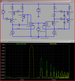
an illustration of the potential performance difference of actually using buffered cascode VAS topology vs the OP' circuit
the models are chosen from Ltspice included parts - may not be the greatest but I used the same in the 2 circuits compared below
changing topology, passives, bias, the circuit on the left is actually operating as a buffered cascoded VAS as explained in Cordell's, Self's books
the right "not_cascode" circuit is the OP's VAS (green fft)
the cascode gives ~ 60 dB lower distortion (yellow fft trace)
the comparison isn't fully debugged, RF stability not compared - the only point I'm trying to show is that "proper" cascode operation is easily distinguished
Attachments
What amps measure better than this?an illustration of the potential performance difference of actually using buffered cascode VAS topology vs the OP' circuit
the models are chosen from Ltspice included parts - may not be the greatest but I used the same in the 2 circuits compared below
changing topology, passives, bias, the circuit on the left is actually operating as a buffered cascoded VAS as explained in Cordell's, Self's books
the right "not_cascode" circuit is the OP's VAS (green fft)
the cascode gives ~ 60 dB lower distortion (yellow fft trace)
the comparison isn't fully debugged, RF stability not compared - the only point I'm trying to show is that "proper" cascode operation is easily distinguished
just showing the VAS in isolation - nonlinear output stage driver load Z will be a limit, if the VAS CCS were capable of performing at this level
what is really wanted is more audio frequency loop gain - which the buffered cascode can also deliver - then 2-pole compensation can cut all amplifier stage's distortion thru increased audio frequency global feedback
also note that my comparison is 20 kHz distrotion - Bob's favorite "simple metric"
a number of amp designs today can manage few 10's to single digit ppm distortion numbers at 1 kHz
Last edited:
Nice work jcx. I have to admit that I have changed the topology just a little more; the 100nF cap now bypasses the 2K7 resistor directly, not 'after' the individual gate stoppers which I had increased to 100Ohm.
In the circuit the topology performs better than either a single transistor or the fixed ref cascode. I'll try some comparissons as well, although it's not my main intent which is to complete this design.
P.S. THD20 is my favourite as well, if it works there, it will work at THD1 certainly. For THD1 I achieved numbers in the 10...100 ppb range with this schematic.
Could it be that this VAS structure sort of cancels the harmonics generated in the VAS CCS at the bottom? That would be one explanation.
LazyCat, when you look at the schematic, what do you think? Ofcourse it's near impossible to tell audio performance from a plain schematic, could you give any hint at the level of 'promising' for this design?
As I remember correctly you were initially inspired by Fetzila type of the amp just to go in a more sophisticated way of doing it for each functional part of the schematic. That is a good way if this sophistication will work in a favour to sound improvement as well.
I really can not tell you how this amp would sound, but I can point out to you in which direction to go by simulation and measuring data. As you already stated distortion harmonic distribution profile (linear decrease of H components) is one of them. Others? Well, try to go to zero phase shift/delay at 100 kHz, slew rate of more than 250 V/us, -3 dB bandwidth at 2 Mhz, more than 100 dB noise floor and you're half way there. The other half is PCB, parts, final assembly etc.
Regards, Andrej
")
As I remember correctly you were initially inspired by Fetzila type of the amp just to go in a more sophisticated way of doing it for each functional part of the schematic. That is a good way if this sophistication will work in a favour to sound improvement as well.
I really can not tell you how this amp would sound, but I can point out to you in which direction to go by simulation and measuring data. As you already stated distortion harmonic distribution profile (linear decrease of H components) is one of them. Others? Well, try to go to zero phase shift/delay at 100 kHz, slew rate of more than 250 V/us, -3 dB bandwidth at 2 Mhz, more than 100 dB noise floor and you're half way there. The other half is PCB, parts, final assembly etc.
Regards, Andrej
Thanks, in other words: Employ standard practice
Your design criteria are no different from mine.just showing the VAS in isolation - nonlinear output stage driver load Z will be a limit, if the VAS CCS were capable of performing at this level
what is really wanted is more audio frequency loop gain - which the buffered cascode can also deliver - then 2-pole compensation can cut all amplifier stage's distortion thru increased audio frequency global feedback
also note that my comparison is 20 kHz distrotion - Bob's favorite "simple metric"
a number of amp designs today can manage few 10's to single digit ppm distortion numbers at 1 kHz
Jcx, its exactly what the OP circuit does, not only does it lower the miller effect (less so than conventional cascode) but it it increases loop gain considerably and its the main reason it performs so well. Simulations with this circuit is awkward as the subthreshold region in mosfet models are hideous and I personally wouldnt even try simulation interpretation. Using a similar setup Im able to improve vas performance to near the same league of using a buffered hawksford cascoded bjt vas without all the stabilty hiccups. Parts selection is very important.
I really can not tell you how this amp would sound, but I can point out to you in which direction to go by simulation and measuring data. As you already stated distortion harmonic distribution profile (linear decrease of H components) is one of them. Others? Well, try to go to zero phase shift/delay at 100 kHz, slew rate of more than 250 V/us, -3 dB bandwidth at 2 Mhz, more than 100 dB noise floor and you're half way there. The other half is PCB, parts, final assembly etc.
Regards, Andrej
Those are very average parameters to what can be achieved with the circuit idea shown here, we are nearing 2012 and need rather than fall back to 40 year old circuits ideas to look at new ones.
- Status
- This old topic is closed. If you want to reopen this topic, contact a moderator using the "Report Post" button.
- Home
- Amplifiers
- Solid State
- "State-Of-MOS": 200W Ultra Low Distortion Pure FET Amplifier