bear said:the two transistors refers to the "Allison" transistors.
I don't think that Allison's original intent was to provide feedback for anything but the bias.
So, the question is then, does the technique of not limiting the the HF response so that it works only at near DC provide a reduction of distortion for the output stage, and if so, how much?
Should be easy enough to simulate by throwing in the cap and taking it out of the original simple circuit?
And, is it then just a variation of Hawksford or not??

keantoken, nice going! Have you built any circuits into real world units or are you just doing the simulations so far??
Btw, you ought to be able to get into a top notch engineering school without any trouble... fyi. Email me if you need any insights into how to do that...
_-_-bear
Oops, I made a mistake. Which transistors are you referring to in the STAX schematic? Looking back again, I really don't see an Allison. I thought that Q139 and Q140 were but after looking again, they are actually overpower protection. Q113 and Q114 look like and Allison at first but they are actually a fancy Vbe multiplier (I wouldn't qualify this as an Allison but I have no access to Allison's original article). Q107-Q110 I have seen in a patent somewhere, but no Allison.
"tricking" the Allison into working only at near DC I don't think will have any benefit since the caps will also isolate the high frequency feedback signals. Thus, the Allison would simply function as a normal Vbe multiplier, giving a constant bias voltage, and giving similar distortion specs, except for at low frequencies.
The Allison works so well because it adjusts the bias voltage to make sure that bias current is always the same. The result of this is that the bias voltage is not constant. If you look at the bias voltage in simulation, it is actually a close 2nd harmonic of the input signal.
Personally, I think the Allison would make a PERFECT current amplifier for a chip/discrete amp. Distortion would probably be nearly as low as with the opamp itself. Someone could certainly make a project out of this.
I have built a few circuits on breadboard, including a cap charger of my own design (what fun!
 ), and a very annoying oscillator that gave me extreme ear fatigue (again of my own design, which was quite pitiful). Maybe that's one I could sell. I've built one audio amplifier and have been messing with it since, but only once was I able to make it truly sparkle. No idea why.
I've activated the Email button at the bottom of my post. I am interested in what ideas you have... Tell me if you want me to Email you first.
About being a variation of Hawksford, it looks similar but accomplishes the same goal indirectly. It gets its error signal from the bias current rather than the bias voltage (which is affected by the base current of the output devices). Perhaps we should compare the Allison and the Hawksford in simulation?
How about adding an error correction loop across Alison buffer for further reduction in THD?
Now that I understand error correction a bit better, I realize this might be a good idea. But there are still several things to consider, like PCB design (without this, nothing is good enough). Do you think you could post an example of the circuit you have in mind? I'm not sure what you mean here.
I think adding error correction would only either increase distortion or keep it at the same level. The only benefit I think would be to give the Allison more linear input impedance (this is actually a significant one - it might be worth it in certain situations). It might increase gain but I don't think that is necessary. If we need more power we can just use parallel output devices.
But I still don't know much about error correction, so you will probably prove me wrong.
- keantoken
Hmmmm... I was looking at Q139/140.
I wish I could post the schematic in case anyone cares who is reading along... not sure how to get it from pdf to here... let me try, who knows what will happen.
Current, voltage, does it matter really? The drop across the emitter resistors is a voltage, yes? Or am I completely wrong and confused about what is happening?
So, my question remains, what is the "native" THD of a given circuit (take the basic circuit first) and then the "Allison" THD of the same circuit? The cap should change it from just a "fancy Vbe" (which is what I thought it was supposed to be) to something else...
_-_-bear
Edit: the .pdf is too large to include... tried
Spice simulation
Keantoken,
Thanks for the Allison model - i've been messing with Ltspice for a few months using models made by others and then trying my own. I tried putting the output section of the Leach amp into your model - file attached. I can't get it to work correctly can you help? There is a waver in the sine wave of the output at the zero crossing. The bias also has a blip at the same time location. I've also attached the model of the Leach amp as well for comparison.
Thanks
Ken
Klewis:
You're welcome.
I don't think it is fair to compare the Allison with the Leach because the Allison is optimized for distortion, while it seems the aim of the Leach output was to provide low TIM and high gain.
I got it to work but distortion was quite high. Maybe I did it wrong. Anyways, I don't think it's productive to compare the Allison with every other popular output stage unless it is known for low distortion.
The intent of the Allison is not to provide a constant Vbe, but to provide constant bias current. The voltage across the emitter resistors must be the same at all times. Thus, if current increases in one resistor, the Allison adjusts and makes the current in the other resistor smaller.
I think I've made a mistake in calling the Allison a Vbe multiplier. This is wrong. The Allison could be called an error correction circuit, but more precisely it controls bias current with a feedback loop. It seems that Hawksford's error correction circuitry assumes linear Vbe for the output transistors and corrects only for base current fluctuations (am I right?). The Allison does not take Vbe for granted. Unless Hawksford had a version of this particular circuit before Allison's publication, I can't call it a Hawksford. I believe Allison's idea is unique but I cannot say whether or not he borrowed inspiration from Hawksford (maybe Hawksford was inspired by Allison?).
So in short, I don't think the Allison was Hawksford's idea. But then again I haven't researched this much.
I'm sorry to get bogged down in details but if we don't use correct terms people will be mislead... I have experienced this.
I will simulate the CFP with a standard Vbe multiplier and with an Allison so that we can compare.
- keantoken
You're welcome.
I don't think it is fair to compare the Allison with the Leach because the Allison is optimized for distortion, while it seems the aim of the Leach output was to provide low TIM and high gain.
I got it to work but distortion was quite high. Maybe I did it wrong. Anyways, I don't think it's productive to compare the Allison with every other popular output stage unless it is known for low distortion.
Hmmmm... I was looking at Q139/140.
I wish I could post the schematic in case anyone cares who is reading along... not sure how to get it from pdf to here... let me try, who knows what will happen.
Current, voltage, does it matter really? The drop across the emitter resistors is a voltage, yes? Or am I completely wrong and confused about what is happening?
So, my question remains, what is the "native" THD of a given circuit (take the basic circuit first) and then the "Allison" THD of the same circuit? The cap should change it from just a "fancy Vbe" (which is what I thought it was supposed to be) to something else...
_-_-bear
The intent of the Allison is not to provide a constant Vbe, but to provide constant bias current. The voltage across the emitter resistors must be the same at all times. Thus, if current increases in one resistor, the Allison adjusts and makes the current in the other resistor smaller.
I think I've made a mistake in calling the Allison a Vbe multiplier. This is wrong. The Allison could be called an error correction circuit, but more precisely it controls bias current with a feedback loop. It seems that Hawksford's error correction circuitry assumes linear Vbe for the output transistors and corrects only for base current fluctuations (am I right?). The Allison does not take Vbe for granted. Unless Hawksford had a version of this particular circuit before Allison's publication, I can't call it a Hawksford. I believe Allison's idea is unique but I cannot say whether or not he borrowed inspiration from Hawksford (maybe Hawksford was inspired by Allison?).
So in short, I don't think the Allison was Hawksford's idea. But then again I haven't researched this much.
I'm sorry to get bogged down in details but if we don't use correct terms people will be mislead... I have experienced this.
I will simulate the CFP with a standard Vbe multiplier and with an Allison so that we can compare.
- keantoken
I'm too slow to know off the top of my head what is going on here... my first inclination is that Allison intended only LF for bias control, not EC.
Then I am wondering what the diff is between your version of Allison and Hawksford, except the source point of the EC's feedback signal.
No time to read and look right now... someone else reading doubtless has this insight off the top of their head?
That would be nice.
_-_-bear
Then I am wondering what the diff is between your version of Allison and Hawksford, except the source point of the EC's feedback signal.
No time to read and look right now... someone else reading doubtless has this insight off the top of their head?
That would be nice.
_-_-bear
I've been playing with something similar. Emitter coupled
base followers with two emitter voltage offset between.
Backwards looking error correction.... Etc Etc...
I've been calling the topology a "Forklift".
Coping with some of challenges regarding input impedance
across the full audio frequency. The "Allison" transistor is
the top end of a cascode, The input signal is the lower
end of that same cascode. Any current change needed
to drive the next device will have to be conducted by the
input emitter(s). It can't come from the CSS, where else
is the necessary current delta gonna come from?
So buffers are needed. Matters little if these come before
the emitter junctions or after. As long as the input isn't
directly driving the output devices (through the emitter)...
Not as you see in my oversimplified drawing below.
My inspiration originated with Nelson's "Aleph", not with
Allison. But seems to have devolved along similar lines...
This was an early version of the concept before buffers
complicated it. And using bootstraps rather than CCS....
.ASC files for this schematic and later versions can be
found over in my thread "Possible improvements for
Aleph" in the Pass Labs section of the forum.
Attachments
Neat.
I wonder how the bootstraps affect Allison stability.
If you want to experiment, you could try connecting R2 between the Allison emitters and the output. At maximum current output, the voltage between these two points is around 700mV. 2A into 8ohms is 16V. So 16.7/47k=355uA. In order to have the same input impedance, you would need to use a 1.9k resistor. This idea seems interesting to me. I think that the input impedance would be affected by the load impedance (although it already is to an extent), and any load changes would show up in the input impedance proportionally, since the load current will determine the voltage across R2. At first this seems like it doesn't have any benefits, but I wonder what advantages it has?
- keantoken
kenpeter said:What happens if you move your "rush" transistors Q35 Q36
up an emitter, base reference the emitters of Q31 Q32.
Does this added .66V collector working voltage seen at all
four corners of the diamond help?
I am not sure but I think I know what you mean.
Q35 and Q36 are cascodes. I have tried using them like you say, and I have also tried referencing them from the bases of Q16 and Q29 but the present arrangement works the best distortion-wise and is the most stable.
- keantoken
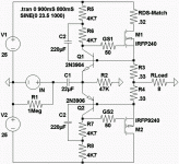
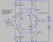
For those of you still watching this, one more variation on the Allison:
Here I worked on the original design in order to overcome the limits of the more complex versions regarding distortion.
There is one big error here:
The drivers should have at least a diode in series with their emitters. This is so that the Allison has enough voltage drop across its B-C junction to function properly. This version is perfect for Darlington outputs. It also gives lower distortion. But it was very hard to get stable even in the simulator. /:
Just for your interest.
- keantoken
An externally hosted image should be here but it was not working when we last tested it.
Here I worked on the original design in order to overcome the limits of the more complex versions regarding distortion.
There is one big error here:
The drivers should have at least a diode in series with their emitters. This is so that the Allison has enough voltage drop across its B-C junction to function properly. This version is perfect for Darlington outputs. It also gives lower distortion. But it was very hard to get stable even in the simulator. /:
Just for your interest.
- keantoken
You just need to Schade back the error correction gains.
That they might have well defined voltage gain limits
independent of weather the load is cooperating or not,
parasitic phase shifts, etc....
Don't leave them entirely open loop, or they overcorrect.
Possibly not in real life, but definitely in the simulator.
Better for avoiding oscillation and those weird unexplainable
LTspice moments... Better behaved in clipping recovery and
class AB if you choose to bias that low.
kenpeter said:You just need to Schade back the error correction gains.
That they might have well defined voltage gain limits
independent of weather the load is cooperating or not,
parasitic phase shifts, etc....
Don't leave them entirely open loop, or they overcorrect.
Possibly not in real life, but definitely in the simulator.
Better for avoiding oscillation and those weird unexplainable
LTspice moments... Better behaved in clipping recovery and
class AB if you choose to bias that low.
What do you mean be "schade"?
If I knew what that word meant I could understand the rest of your paragraph.Maybe you have seen this already, but the four diodes here is a simple way to prevent overcurrent:
- keantoken
Here is an interesting update.
I've found that the Hfe of the Allison transistors is not a significant factor contributing to distortion. If you want my "proof", simulate using BC547C/557C for the Allison, and then simulate using 2N5769/5771 (if you have them, you can also try the THAT package models) for the same. You should see an insignificant decrease in distortion and increase in bandwidth.
What this means is that for the Allison, the THAT packages should actually be the best possible thing to use. Not only will you get higher bandwidth, but since there is less gain, it should be more stable.
What this means is that Vbe vs Ic is the most important consideration rather than Hfe, so we can get away with low-gain transistors here for better bandwidth and better stability (those two don't often come together).
Next
Given you use the same output devices and drivers, along with the same bias currents, there is virtually no advantage in using the CFP over the Darlington. (I digress; there is actually an insignificant decrease in distortion when using the darlington - by .000022%!).
If you want to squeeze even more bandwidth out of the Allison, you should use a Darlington output configuration, since it is less affected by its own parasitic miller capacitance. Although I don't know why you would need it for the audio band.
- keantoken
Posted by CBS240...
These are very good indeed but the cost is not. You get what you pay for I suppose. Although they have high ft and very low noise, the current gain is only about 80-90. The ones I have measure about 86. This and the fact that Vce is only 36V is why I used them in a constant power differential. Excellent results, btw. Try to keep Ic max to a few milliamps or so. Also there is no need for emitter degeneration. After all, that is what you pay for, eh? I'm not sure I could have gotten these waveforms from this ( TOP) ugly looking thing without using them as the amplifying devices. (Output is actually a bridged output so the top photos show each output. Bottom ones is what the load sees.) If they just weren't so darned expensive, I would use them for just about everything possibe. Hey, they still don't compare in price when buying a duel matched J-fet....if you can find them.
I've found that the Hfe of the Allison transistors is not a significant factor contributing to distortion. If you want my "proof", simulate using BC547C/557C for the Allison, and then simulate using 2N5769/5771 (if you have them, you can also try the THAT package models) for the same. You should see an insignificant decrease in distortion and increase in bandwidth.
What this means is that for the Allison, the THAT packages should actually be the best possible thing to use. Not only will you get higher bandwidth, but since there is less gain, it should be more stable.
What this means is that Vbe vs Ic is the most important consideration rather than Hfe, so we can get away with low-gain transistors here for better bandwidth and better stability (those two don't often come together).
Next
Given you use the same output devices and drivers, along with the same bias currents, there is virtually no advantage in using the CFP over the Darlington. (I digress; there is actually an insignificant decrease in distortion when using the darlington - by .000022%!).
If you want to squeeze even more bandwidth out of the Allison, you should use a Darlington output configuration, since it is less affected by its own parasitic miller capacitance. Although I don't know why you would need it for the audio band.
- keantoken
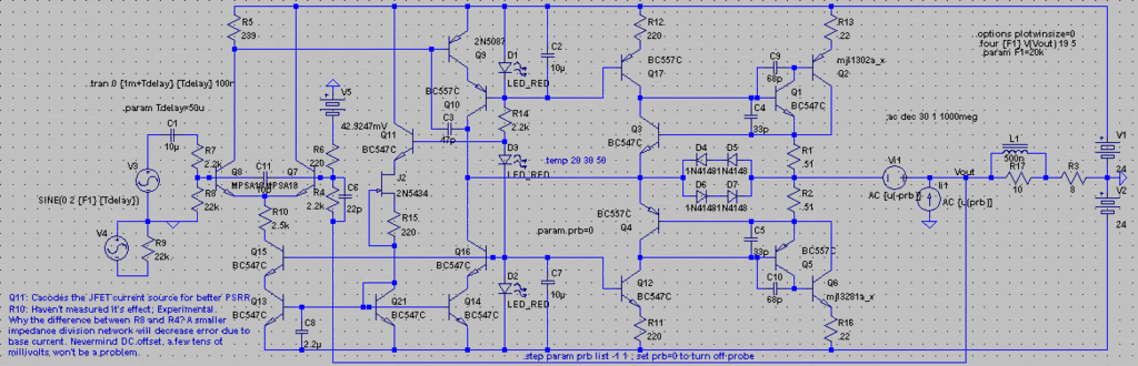
Another development
Someone suggested I do some sort of nested error correction type thing, and I think this is the realization of that idea.
This simple circuit is amazing.
Simulated distortion figures are (with a perfect input voltage source):
THD @ 100Hz, 37.6V pk-pk into 8 ohms = .000013%
THD @ 1KHz, 37.6V pk-pk into 8 ohms = .000013%
THD @ 20KHz, 37.6V pk-pk into 8 ohms = .000022%
THD @ 100KHz, 37.6V pk-pk into 8 ohms = .000125%
Implications:
The circuit has inherently high input impedance, but it is very capacitive. Look at the input impedance curve (note, if the Y scale was logarithmic, it would be a straight downward slanting line):
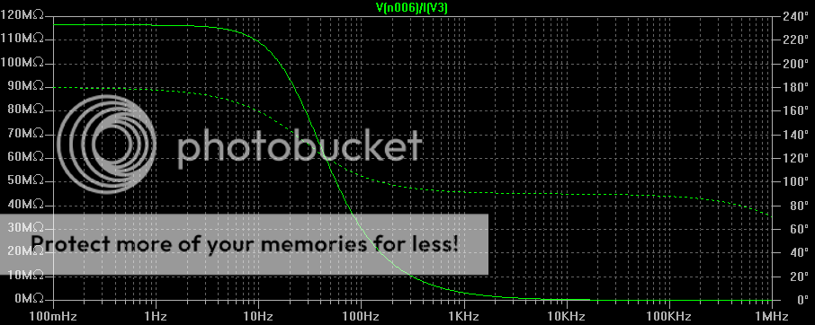
That is, 3.13megaohms at 1KHz, 313Kohms at 10KHz, and 31.3Kohms at 100KHz. Impedance below 1Hz is about 116Megaohms.
Input impedance linearity test:
These simulations are performed with a 10k input impedance to test the linearity of the Allison-based circuit with high source impedances.
THD @ 100Hz, 37.6V pk-pk into 8 ohms = .000593%
THD @ 1KHz, 37.6V pk-pk into 8 ohms = .003409%
THD @ 20KHz, 37.6V pk-pk into 8 ohms = .068963%
THD @ 100KHz, 37.6V pk-pk into 8 ohms = .386746%
So all in all, this circuit is the best so far of my Allison variants - if you have a good source. Without a good source, THD will be strongly correlated with frequency. I also suspect this one is very stable - moreso than any other of my variations, although I haven't tested this.
- keantoken
Someone suggested I do some sort of nested error correction type thing, and I think this is the realization of that idea.
This simple circuit is amazing.
Simulated distortion figures are (with a perfect input voltage source):
THD @ 100Hz, 37.6V pk-pk into 8 ohms = .000013%
THD @ 1KHz, 37.6V pk-pk into 8 ohms = .000013%
THD @ 20KHz, 37.6V pk-pk into 8 ohms = .000022%
THD @ 100KHz, 37.6V pk-pk into 8 ohms = .000125%
Implications:
The circuit has inherently high input impedance, but it is very capacitive. Look at the input impedance curve (note, if the Y scale was logarithmic, it would be a straight downward slanting line):
That is, 3.13megaohms at 1KHz, 313Kohms at 10KHz, and 31.3Kohms at 100KHz. Impedance below 1Hz is about 116Megaohms.
Input impedance linearity test:
These simulations are performed with a 10k input impedance to test the linearity of the Allison-based circuit with high source impedances.
THD @ 100Hz, 37.6V pk-pk into 8 ohms = .000593%
THD @ 1KHz, 37.6V pk-pk into 8 ohms = .003409%
THD @ 20KHz, 37.6V pk-pk into 8 ohms = .068963%
THD @ 100KHz, 37.6V pk-pk into 8 ohms = .386746%
So all in all, this circuit is the best so far of my Allison variants - if you have a good source. Without a good source, THD will be strongly correlated with frequency. I also suspect this one is very stable - moreso than any other of my variations, although I haven't tested this.
- keantoken
Yeah, but the diamond is now 4 full silicon emitter drops wide....
Half an ohm output impedance.... Full ohm or more if biased AB...
This just might be Germanium comparator territory...
Still need .models with the correct VBE.
Or somehow throw an extra silicon emitter into closing the diamond.
Half an ohm output impedance.... Full ohm or more if biased AB...
This just might be Germanium comparator territory...
Still need .models with the correct VBE.
Or somehow throw an extra silicon emitter into closing the diamond.
- Status
- This old topic is closed. If you want to reopen this topic, contact a moderator using the "Report Post" button.
- Home
- Amplifiers
- Solid State
- Simulation Analysis of several unique Allison-based output stages.