Actually, I have one design where the R085's Vgs is a better fit.

Phew
Nelson how did you do the Min H2 measurement ? Load line cancellation ?
Load line cancellation. Vary the Ids and Vds.
That makes sense, and I alluded to that in my post, i.e. attenuated/offset Vgs and/or source degeneration.In the solid-state tube, we are not modifying the SJDP120R085 JFET so much as we are using it in an application. We use a 6L6 data sheet to determine the characteristic curves.
I think creating a SS version of all tubes is a good idea, but replacing tube amplifiers with equivalent-performing SS designs is even better. And that's just what I'm working on.
The Infineon IJW120R100T1 offers some rather unique possibilities with their large negative gate voltages Vgs for 2 amperes of quiescent current.
It enables a simple way to get DC-coupled inputs on a SoZ v.7, since it will accommodate the constant current source or large air-cored coil "below" the Vgs of the Jfets. With an output transformer with trifilar or quadfilar windings (SoZ v.7T) it would enable DC-coupled inputs and a very easy DC-free SUSY feedback arrangement.
There are many more unique opportunities with this extremely large negative gate to source voltage.
Cheers,
Johannes
There are many more unique opportunities with this extremely large negative gate to source voltage.
What I like about large negative Vgs is that it makes for good simple cascodes,
as the voltage across the cascoded device is high enough that its capacitance
is brought down to lower values and its transconductance will be higher.
Also, it provides room for plenty of degeneration, improving the impedance of
simple current sources.
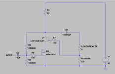
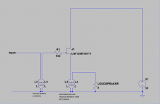
Here are two possible uses of the large negative Vgs of the Infineon IJW100R100T or similar SiC Jfet.
The modulated cascode would be quite useless with a normal "pentod-ish" mosfet since it does not care much for any voltage-variation on the drain. Within the ohmic linear region of SITs Triodes or large-ohmic-region devices like the IRFP7430 you can use modulated cascode and similar cascode-feedback techniques to explore your load-line just like Nelson Pass does in the Zen V.9 (Lovoltech power-Jfet).
The aircored output transformer is quite obvious. The output transformer can be an simple single winding large inductance, a bifilar 1:1 transformer or autoformer or an tri/quadfilar step-up aircored transformer or autoformer. In some examples you will need an output DC voltage blocking capacitor.
Just some ideas for those of you who wants to play with these exciting power-Jfets but feel a little put of by their large negative Vgs.
Cheers,
Johannes
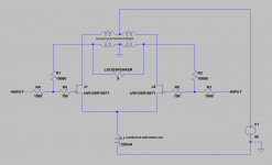
This was my idea I wrote about yesterday in this thread (SoZ V.7-T)
I just wanted to post a simple schematic to better explain my idea.
Sadly I don't own any of these devices (yet) so this is just some theoretical unique possibilities these devices presents with their large negative Vgs.
Cheers,
Johannes
"NP-What I like about large negative Vgs is that it makes for good simple cascodes"
Yes these depletion mode devices are designed to work with LV mosfets in cascode configuration.
I've had some Lovotech JFETs hanging around since 2007 - it would be interesting to mount one on a spreader and pair it up with one of the Infineon SiC JFETs.
Yeah me too.
I've been meaning to put them to use for a while. I'll probably just use some N Channel Lateral Mosfets as cascode.
I'm getting very close to the point of just forgetting about this on going desire to find the holy grail.
There is so much that can be done with what we already have.
I'm getting very close to the point of just forgetting about this on going desire to find the holy grail.
There is no holy grail of amplifier and transistor design, but there is an ongoing development.
Silicon is a better semiconductor material then Germanium and Silicon Carbide is better then Silicon, Gallium Nitride is better then those three and Graphene seems to promise a revolution in semiconductor design. I would love to see Graphen SITs in TO-247 packages sold for a few dollars a piece from Mouser.

A SiC Jfet or the latest breed of fun mosfets from IR, IXYS and Fairchild is in many ways much better parts then the old IRFP240/150/044/etc or lateral devices.
I have been eyeballing these for some time now:
http://www.mouser.se/pdfdocs/PreliminaryTO220GANDatasheetPGA26C09DV.pdf
Gallium Nitride semiconductors seem to have huge amounts of transconductance for very low amounts of gate capacitance. Every transfer-curve I have seen is shows a very high tranconductance and linear device.
http://www.mouser.com/ds/2/692/GS66516T%20DS%20Rev%20160318-913407.pdf
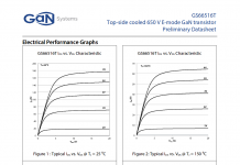
I am very tempted to buy a few of these and clamp them to a solid block of copper, to see what can be done with these small surface-mount parts.
They have quite spectacular electrical properties.
Cheers,
Johannes
A GaN GS66516T (link in previous post) has a low Ciss of only 520 pF, a thermal resistance from junction to case of 0.3 C/W and seems to have transconductance around 50 S. A 9 x 7,64 mm surface area is not very small compared to a TO-220 package. With such a low thermal resistance I guess we can run it with a continuous 20 watt heat dissipation if clamped to a solid copper bar or block.
Perfect for Schade Feedback (low Ciss enables usable feedback resistor values) and cascoding for more power.
Cheers,
Johannes
Perfect for Schade Feedback (low Ciss enables usable feedback resistor values) and cascoding for more power.
Cheers,
Johannes
The High transconductance/low capacitance is both a blessing and a curse. GaN HEMTs make wonderful microwave devices - they already have a significant niche in that market. Getting them to shut up in an audio context might prove difficult, like those tubes that are rumored to "oscillate in the box". I would love to mess with some of the GaN mosfets from EPD, but they are in these horrible flip-chip packages that make them almost impossible for amateur use. They are probably finding a home in high density, high frequency DC-DC converters
The GaN GS66516T is not a HEMT. It is "normal" enhanced mode Mosfet. Iwould probably start with a 0.25w metalfilm 1000 ohm gate-stopper to play safe.
I have been drooling at the GaN HEMT too, but I am afraid of the "oscillate in the box" part you write about, and they are not exactly cheap.
I don't think they are impossible for amateur use. A 9 x 7 mm package is not much smaller then an TO220. Yes, I will probably have to use a magnifying glass when soldering the gate-stopper to the gate-pad and a small piece of wire to the drain-pad.
The large source-pad will be pressed hard against a piece of copper plate or solid copper bar.
I think its fine as long as you don't plan on building a 200 watt pushpull amp with many of these devices paralleled. For FAB amateur use I would just clamp it down hard with a simple clamp.
Cheers,
Johannes
I have been drooling at the GaN HEMT too, but I am afraid of the "oscillate in the box" part you write about, and they are not exactly cheap.
but they are in these horrible flip-chip packages that make them almost impossible for amateur use
I don't think they are impossible for amateur use. A 9 x 7 mm package is not much smaller then an TO220. Yes, I will probably have to use a magnifying glass when soldering the gate-stopper to the gate-pad and a small piece of wire to the drain-pad.
The large source-pad will be pressed hard against a piece of copper plate or solid copper bar.
I think its fine as long as you don't plan on building a 200 watt pushpull amp with many of these devices paralleled. For FAB amateur use I would just clamp it down hard with a simple clamp.
An externally hosted image should be here but it was not working when we last tested it.
Cheers,
Johannes
Interesting about the one part - Panasonic has been jawboning about GaN for some time. I didn't realize they had finally coughed up.
We actually tried to use the EPD parts in our lab at work. They would be no sweat for someone with properly stenciled solder paste. good pick and place, and your usual reflow setup, but manually soldering them is almost impossible. We had to take the finished assemblies down to QA and X-ray them to make sure the soldering was ok. Having said that, they worked fine for their intended purpose. I'd take that Panasonic TO-220 any day, parasitic lead inductance and all...
We actually tried to use the EPD parts in our lab at work. They would be no sweat for someone with properly stenciled solder paste. good pick and place, and your usual reflow setup, but manually soldering them is almost impossible. We had to take the finished assemblies down to QA and X-ray them to make sure the soldering was ok. Having said that, they worked fine for their intended purpose. I'd take that Panasonic TO-220 any day, parasitic lead inductance and all...
GaN Systems
My bad.
I see these devices are HEMTs. I thought only the GaN on SiC radar-parts where HEMTs.
As I understand this, these HEMTs need some resistance on all three pins to avoid oscillation. The resistance-values needs to be spread out compared to the capacitance and resistance of the different pins, to avoid creating high Q resonant circuits at the same frequencies or even harmonics of those frequencies. It is doable, but one has to take great care to use low inductance resistors and extremely short leads (SMD resistor soldered directly to the gate etc).
Cheers,
Johannes
- Status
- This old topic is closed. If you want to reopen this topic, contact a moderator using the "Report Post" button.
- Home
- Amplifiers
- Pass Labs
- SemiSouth boiler room
